Features: • Double data rate architecture: two data transfers per clock cycle
• Bidirectional data strobe (DQS) is transmitted and received with data, to be used in capturing data at the receiver
• DQS is edge-aligned with data for reads and is center-aligned with data for writes
• Differential clock inputs (CK and CK)
• Four internal banks for concurrent operation
• Data mask (DM) for write data
• DLL aligns DQ and DQS transitions with CK transitions
• Commands entered on each positive CK edge; data and data mask referenced to both edges of DQS
• Burst Lengths: 2, 4, or 8
• CAS Latency: (1.5), 2, 2.5, 3
• Auto Precharge option for each burst access
• Auto Refresh and Self Refresh Modes
• 7.8s Maximum Average Periodic Refresh Interval
• 2.5 V (SSTL_2 compatible) I/O
• VDDQ = 2.5 V ± 0.2 V (DDR266A, DDR333)
• VDD = 2.5 V ± 0.2 V (DDR266, DDR333)
• P-TSOP66II-1 packagePinout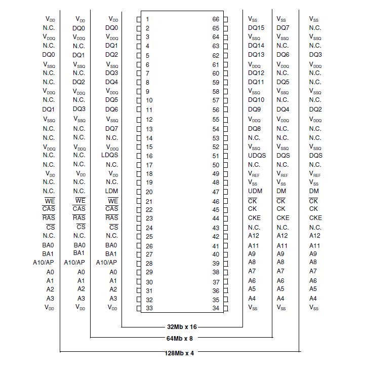 Description
The 512Mbit Double Data Rate SDRAM HYB25D512160AT-7 is a high-speed CMOS, dynamic random-access memory containing 536,870,912 bits. It is internally configured as a quad-bank DRAM.
The 512Mbit Double Data Rate SDRAM HYB25D512160AT-7 uses a double-data-rate architecture to achieve high-speed operation. The double data rate architecture is essentially a 2n prefetch architecture with an interface designed to transfer two data words per clock cycle at the I/O pins. A single read or write access for the 512Mbit Double Data Rate SDRAM effectively consists of a single 2n-bit wide, one clock cycle data transfer at the internal DRAM core and two corresponding n-bit wide, one-half-clock-cycle data transfers at the I/O pins.
A bidirectional data strobe (DQS) is transmitted externally, along with data, for use in data capture at the receiver. DQS is a strobe transmitted by the DDR SDRAM HYB25D512160AT-7during Reads and by the memory controller during Writes. DQS is edge-aligned with data for Reads and center-aligned with data for Writes.
The 512Mbit Double Data Rate SDRAM HYB25D512160AT-7 operates from a differential clock (CK and CK; the crossing of CK going HIGH and CK going LOW is referred to as the positive edge of CK). Commands (address and control signals) are registered at every positive edge of CK. Input data is registered on both edges of DQS, and output data is referenced to both edges of DQS, as well as to both edges of CK.
Read and write accesses to the DDR SDRAM HYB25D512160AT-7 are burst oriented; accesses start at a selected location and continue for a programmed number of locations in a programmed sequence. Accesses begin with the registration of an Active command, which is then followed by a Read or Write command. The address bits registered coincident with the Active command are used to select the bank and row to be accessed. The address bits registered coincident with the Read or Write command are used to select the bank and the starting column location for the burst access.
The DDR SDRAM HYB25D512160AT-7 provides for programmable Read or Write burst lengths of 2, 4 or 8 locations. An Auto Precharge function may be enabled to provide a self-timed row precharge that is initiated at the end of the burst
access.
As with standard SDRAMs HYB25D512160AT-7, the pipelined, multibank architecture of DDR SDRAMs allows for concurrent operation, thereby providing high effective bandwidth by hiding row precharge and activation time.
An auto refresh mode is provided by HYB25D512160AT-7 along with a power-saving power-down mode. All inputs are compatible with the JEDEC Standard for SSTL_2. All outputs are SSTL_2, Class II compatible.
Note: The functionality described and the timing specifications included in this data sheet are for the DLL Enabled mode of operation.

 HYB25D512160AT-7 Data Sheet