Features: • Organization : 1M x 16
• Power Supply Voltage : 2.7~3.3V
• Three state output and TTL Compatible
• Package Type : 48-FBGA-6.00x8.00 mm2
• Address Acess Time : 70nsPinout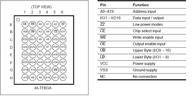 Specifications
| Symbol |
Parameter |
Ratings |
Unit |
| VIN,VOUT |
Voltage on any pin relative to Vss |
-0.2 to Vcc+0.3 |
V |
| Vcc |
Voltage on Vcc supply relative to Vss |
-0.2 to 3.6 |
V |
| PD |
Power Dissipation |
1.0 |
W |
| TSTG |
Storage Temperature |
-65 to 150 |
°C |
| Toper |
Operating Temperature |
-25 to 85 |
°C |
DescriptionThe IC66LV10016AL is a family of low voltage, low power 16Mbit static RAM organized as 1M-words by 16-bit,designed with PseudSRAM technology,fabricated with CMOS process technology.
The IC66LV10016AL is designed specific ally for low-power applications such as mobile cellular phones, personal digital assistants and other battery-operated products.The operation modes are determined by a combination of the device control inputs CE , ZZ , LB , UB ,WE and OE . Each mode is summarized in the function table.
A write operation of the IC66LV10016AL is executed whenever the low level WE overlaps with the low level LB and/or UB and the low level CE and the high level ZZ . The address (A0~A19) must be set up before the write cycle and must be stable during entire cycle. A read operation is executed by setting WE at a high level and OE at a low level while LB and/or UB and CE are in an active state, ZZ is in a inactive state. When setting LB at the high level and other controls are in an active stage, upper-byte is selected for read and write operations, and lower-byte is not selected. When setting UB at a high level and other pins are in an active stage, lower-byte is selected and upper-byte is not.
When setting LB and UB at a high level or CE and ZZ at a high level or ZZ at a low level, the chip is in a non-select mode. In this mode, the output stage is in a high-impedance state, allowing OR-tie with other chips.
When OE is at a high level, the output stage is in a highimpedance

 IC66LV10016AL Data Sheet