ICS508

Features: • Packaged as 8 pin SOIC or die• Separate VDD supplies allow voltage translation• Clock frequency of 0 - 250 MHz• Duty cycle of 45/55• Operating voltages of 2.375 to 5.5 V• Tri-state output for board level testing• 24 mA drive capability• I...

product image

ICS508 Picture
SeekIC No. : 004370786 Detail

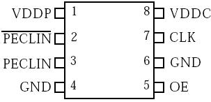
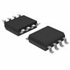
ICS508: Features: • Packaged as 8 pin SOIC or die• Separate VDD supplies allow voltage translation• Clock frequency of 0 - 250 MHz• Duty cycle of 45/55• Operating voltages of 2...
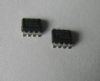
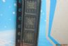
floor Price/Ceiling Price

Part Number:
ICS508
Supply Ability:
5000

Price Break

  • Qty
  • 1~5000
  • Unit Price
  • Negotiable
  • Processing time
  • 15 Days
Total Cost: $ 0.00

SeekIC Buyer Protection PLUS - newly updated for 2013!

  • Escrow Protection.
  • Guaranteed refunds.
  • Secure payments.
  • Learn more >>

Month Sales

268 Transactions

Rating

evaluate  (4.8 stars)

Upload time: 2024/5/18

Payment Methods

All payment methods are secure and covered by SeekIC Buyer Protection PLUS.

Notice: When you place an order, your payment is made to SeekIC and not to your seller. SeekIC only pays the seller after confirming you have received your order. We will also never share your payment details with your seller.
Product Details

Description


Features:

• Packaged as 8 pin SOIC or die
• Separate VDD supplies allow voltage translation
• Clock frequency of 0 - 250 MHz
• Duty cycle of 45/55
• Operating voltages of 2.375 to 5.5 V
• Tri-state output for board level testing
• 24 mA drive capability
• Industrial temperature version available
• Advanced, low power CMOS process


Pinout

  Connection Diagram


Specifications

Parameter Conditions
Minimum
Typical
Maximum
Units
Supply Voltage, VDD Referenced to GND
7
V
Inputs Referenced to GND
-0.5
VDD+0.5
V
Clock Output Referenced to GND
-0.5
VDD+0.5
V
Ambient Operating Temperature  
0
70
ICS512MI only
-40
85
Soldering Temperature Max of 10 seconds
260
Storage temperature  
-65
150


Description

The ICS508 is the most cost effective way to generate a high quality, high frequency CMOS clock output from a PECL clock input.

The ICS508 has separate VDD supplies for the PECL input buffer and the output buffer allowing different voltages to be used. For example, the input clock could use a 3.3 V supply while the output operates from 2.5 V.

The device has an Output Enable pin that tri-states the clock output when the OE pin is taken low.

The ICS508 is a member of the ClockBlocks™ family of devices.


Customers Who Bought This Item Also Bought

Margin,quality,low-cost products with low minimum orders. Secure your online payments with SeekIC Buyer Protection.
Prototyping Products
DE1
Optoelectronics
Transformers
Cables, Wires
Tapes, Adhesives
803
Computers, Office - Components, Accessories
View more