Features: • Dual differential 3.3V LVPECL outputs
• Selectable crystal oscillator interfaceor LVCMOS/LVTTL TEST_CLK
• Output frequency range: 77.5MHz to 780MHz
• Crystal input frequency range: 14MHz to 40MHz
• VCO range: 620MHz to 780MHz
• Parallel or serial interface for programming counterand output dividers
• Duty cycle: 49% - 51% (N > 1)
• RMS period jitter: 2.0ps (typical)
• RMS phase jitter at 155.52MHz, using a 38.88MHz crystal(12KHz to 20MHz): 2.5ps (typical)Phase noise: 155.52MHz (typical), using a 38.88MHz crystal
Offset Noise Power
100Hz .................. -90.5 dBc/Hz
1KHz ................ -114.2 dBc/Hz
10KHz ................ -123.6 dBc/Hz
100KHz ................ -128.1 dBc/Hz
• 3.3V supply voltage
• Lead-Free/Annealed package available
• 0°C to 70°C ambient operating temperature
ApplicationPOWER AND GROUNDING
Place the decoupling capacitors C14 and C15, as close as possibleto the power pins. If space allows, placement of the decoupling capacitor on the component side is preferred. This can reduce unwanted inductance between the decoupling capacitor and the power pin caused by the via. Maximize the power and ground pad sizes and number of vias apacitors. This can reduce the inductance between the power and ground planes and the component power and ground pins. The RC filter consisting of R7, C11, and C16 should be placed as close to the VCCA pin as possible.
CLOCK TRACES AND TERMINATION
Poor signal integrity can degrade the system performance or cause system failure. In synchronous high-speed digital systems, the clock signal is less tolerant to poor signal integrity than other signals. Any ringing on the rising or falling edge or excessive ring back can cause system failure. The shape of the trace and the trace delay might be restricted by the available space on the board and the component location. While routing the traces, the clock signal traces should be routed first and should be locked prior torouting other signal traces.
• The differential 50Ω output traces should have thesame length.
• Avoid sharp angles on the clock trace. Sharp angleturns cause the characteristic impedance to change onthe transmission lines.
• Keep the clock traces on the same layer. Whenever possible,avoid placing vias on the clock traces. Placementof vias on the traces can affect the trace characteristicimpedance and hence degrade signal integrity.
• To prevent cross talk, avoid routing other signal traces inparallel with the clock traces. If running parallel traces isunavoidable, allow a separation of at least three tracewidths between the differential clock trace and the othersignal trace.
• Make sure no other signal traces are routed between theclock trace pair.
• The matching termination resistors should be located asclose to the receiver input pins as possible.
Pinout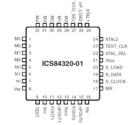 Specifications
1. Power Dissipation.
The total power dissipation for the ICS84320-01 is the sum of the core power plus the power dissipated in the load(s).
The following is the power dissipation for VCC = 3.3V + 5% = 3.465V, which gives worst case results.
NOTE: Please refer to Section 3 for details on calculating power dissipated in the load.
• Power (core)MAX = VCC_MAX * IEE_MAX = 3.465V * 155mA = 537.08mW
• Power (outputs)MAX = 30.2mW/Loaded Output pair
If all outputs are loaded, the total power is 2 * 30.2mW = 60.4mW
Total Power_MAX (3.465V, with all outputs switching) = 537.08mW + 60.4mW = 597.5mW
2. Junction Temperature.
Junction temperature, Tj, is the temperature at the junction of the bond wire and bond pad and directly affects the reliability of the
device. The maximum recommended junction temperature for HiPerClockSTM devices is 125°C.
The equation for Tj is as follows: Tj = JA * Pd_total + TA
Tj = Junction Temperature
JA = Junction-to-Ambient Thermal Resistance
Pd_total = Total Device Power Dissipation (example calculation is in section 1 above)
TA= Ambient Temperature
In order to calculate junction temperature, the appropriate junction-to-ambient thermal resistance JA
must be used. Assuming a
moderate air flow of 200 linear feet per minute and a multi-layer board, the appropriate value is 42.1°C/W per Table 8 below.
Therefore, Tj for an ambient temperature of 70°C with all outputs switching is:
70°C + 0.598W * 42.1°C/W = 95.2°C. This is well below the limit of 125°C.
DescriptionThe ICS84320-01 is a general purpose, dual output Crystal-to-3.3V Differential LVPECL High Frequency Synthesizer and a member of the HiPerClockS™ family of High Performance Clock Solutions from ICS. The ICS84320-01 has a selectable TEST_CLK or crystal inputs. The VCO operates at a frequency range of 620MHz to 780MHz. The VCO frequency is programmed in steps equal to the value of the input reference or crystal frequency. The VCO and output frequency
can be programmed using the serial or parallel interfaces to the configuration logic. The low phase noise characteristics of the ICS84320-01 make it an ideal clock source for 10 Gigabit Ethernet, SONET, and Serial Attached SCSI applications.

 ICS84320-01 Data Sheet