ICS8702BYT

DescriptionThe ICS8702BYT is designed as a low skew, /1, /2 clock generator and a member of the HiPerClockS family of high performance clock solutions from ICS. It is designed to translate any differential signal levels to LVCMOS levels. True or inverting, single-ended to LVCMOS translation can be...

product image

ICS8702BYT Picture
SeekIC No. : 004371088 Detail

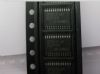
ICS8702BYT: DescriptionThe ICS8702BYT is designed as a low skew, /1, /2 clock generator and a member of the HiPerClockS family of high performance clock solutions from ICS. It is designed to translate any diffe...

floor Price/Ceiling Price

Part Number:
ICS8702BYT
Supply Ability:
5000

Price Break

  • Qty
  • 1~5000
  • Unit Price
  • Negotiable
  • Processing time
  • 15 Days
Total Cost: $ 0.00

SeekIC Buyer Protection PLUS - newly updated for 2013!

  • Escrow Protection.
  • Guaranteed refunds.
  • Secure payments.
  • Learn more >>

Month Sales

268 Transactions

Rating

evaluate  (4.8 stars)

Upload time: 2024/5/1

Payment Methods

All payment methods are secure and covered by SeekIC Buyer Protection PLUS.

Notice: When you place an order, your payment is made to SeekIC and not to your seller. SeekIC only pays the seller after confirming you have received your order. We will also never share your payment details with your seller.
Product Details

Description


Description

The ICS8702BYT is designed as a low skew, /1, /2 clock generator and a member of the HiPerClockS family of high performance clock solutions from ICS. It is designed to translate any differential signal levels to LVCMOS levels. True or inverting, single-ended to LVCMOS translation can be achieved with a resistor bias on the nCLK or CLK inputs, respectively. The effective fanout can be increased from 20 to 40 by utilizing the ability of the outputs to drive two series terminated lines.

It has many features. (1)20 LVCMOS outputs. (2)Output frequency up to 250MHz. (3)150ps bank skew, 200ps output, 250ps multiple frequency skew, 650ps part-to-part skew. (4)Translate any differential input signal (PECL, HSTL, LVDS) to LVCMOS levels withous external bias networks. (5)Translates any single-ended input signal to LVCMOS levels with a resistor bias on nCLK input. (6)Translates any single-ended input signal to inverted LVCMOS levels with a resistor bias on CLK input. (7)LVCMOS/LVTTL control inputs. (8)Bank enable logic allows unused banks to be disabled in reduced fanout applications. And so on.

Some absolute maximum ratings of the ICS8702BYT have been concluded into several points as follow. (1)Its supply voltage would be 4.6V. (2)Its inputs would be from -0.5V to Vdd+0.5V. (3)Its outputs would be from -0.5V to Vdd+0.5V. (4)Its ambient operating temperature range would be from 0°C to 70°C. (5)Its storage temperature range would be from -65°C to 150°C. It should be noted that stresses above those listed in absolute maximum ratings may cause permanent damage to device.

Also some electrical characteristics of the ICS8702BYT are concluded as follow. (1)Its input power supply voltage would be min 3.135V and typ 3.3V and max 3.465V. (2)Its output power supply voltage would be min 3.135V and typ 3.3V and max 3.465V. (3)Its input high voltage would be min 2V and max 3.8V. (4)Its input low voltage would be min -0.3V and max 0.8V. And so on. If you have any question or suggestion or want to know more information please contact us for details. Thank you!


Customers Who Bought This Item Also Bought

Margin,quality,low-cost products with low minimum orders. Secure your online payments with SeekIC Buyer Protection.
Computers, Office - Components, Accessories
Programmers, Development Systems
Soldering, Desoldering, Rework Products
Semiconductor Modules
Undefined Category
View more