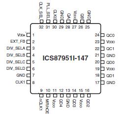
ICS87951I-147

Features: • Fully integrated PLL• Nine single ended 3.3V or 2.5V LVCMOS/LVTTL outputs • Selectable single ended CLK0 or differential CLK1, nCLK1 inputs• The single ended CLK0 input can accept the following input levels: LVCMOS or LVTTL input levels• CLK1, nCLK1 suppor...

product image

ICS87951I-147 Picture
SeekIC No. : 004371104 Detail

ICS87951I-147: Features: • Fully integrated PLL• Nine single ended 3.3V or 2.5V LVCMOS/LVTTL outputs • Selectable single ended CLK0 or differential CLK1, nCLK1 inputs• The single ended CLK0...

floor Price/Ceiling Price

Part Number:
ICS87951I-147
Supply Ability:
5000

Price Break

  • Qty
  • 1~5000
  • Unit Price
  • Negotiable
  • Processing time
  • 15 Days
Total Cost: $ 0.00

SeekIC Buyer Protection PLUS - newly updated for 2013!

  • Escrow Protection.
  • Guaranteed refunds.
  • Secure payments.
  • Learn more >>

Month Sales

268 Transactions

Rating

evaluate  (4.8 stars)

Upload time: 2025/12/5

Payment Methods

All payment methods are secure and covered by SeekIC Buyer Protection PLUS.

Notice: When you place an order, your payment is made to SeekIC and not to your seller. SeekIC only pays the seller after confirming you have received your order. We will also never share your payment details with your seller.
Product Details

Description


Features:

• Fully integrated PLL
• Nine single ended 3.3V or 2.5V LVCMOS/LVTTL outputs
• Selectable single ended CLK0 or differential CLK1, nCLK1 inputs
• The single ended CLK0 input can accept the following input levels: LVCMOS or LVTTL input levels
• CLK1, nCLK1 supports the following input types:LVDS, LVPECL, LVHSTL, SSTL, HCSL
• Output frequency range: 31.25MHz to 200MHz
• VCO range: 250MHz to 500MHz
• External feedback for "zero delay" clock regeneration
• Cycle-to-cycle jitter, RMS: 7ps (maximum)
• Output skew: 270ps (maximum)
• Full 3.3V operating supply at -40°C to 85°C ambient operating temperature
• Full 2.5V operating supply at 0°C to 85°C ambient operating temperature
• Available in both standard and lead-free RoHS compliant packages


Pinout

  Connection Diagram


Specifications

Supply Voltage, VDD .............................................4.6V
Inputs, VI -0.5V to VDDA ..................................+ 0.5 V
Outputs, VO -0.5V to VDDO ..............................+ 0.5V
Package Thermal Impedance, JA ..42.1°C/W (0 lfpm)
Storage Temperature, TSTG .............-65°C to 150°C


Description

The ICS87951I-147 is a low voltage, low skew 1-to-9 Differential-to-LVCMOS/LVTTL Zero Delay Buffer and a member of the HiPerClockS™ family of High Performance Clock Solutions from ICS.The ICS87951I-147 has two selectable clock inputs. The single ended clock input accepts LVCMOS or LVTTL input levels. The CLK1, nCLK1 pair can accept most standard differential input levels. With output frequencies up to 180MHz,the ICS87951I-147 is targeted for high performance clock applications. Along with a fully integrated PLL, the ICS87951I-147 contains frequency configurable outputs and an external feedback input for regenerating clocks with "zero delay".


Customers Who Bought This Item Also Bought

Margin,quality,low-cost products with low minimum orders. Secure your online payments with SeekIC Buyer Protection.
Audio Products
LED Products
Computers, Office - Components, Accessories
Circuit Protection
Isolators
View more