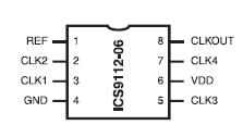
Features: • Zero input - output delay• Frequency range 25 - 75 MHz (3.3V), 30-90MHz (5.0V)• Less than 200 ps Jitter between outputs• Skew controlled outputs• Skew less than 250 ps between outputs• Available in 8 or 16 pin versions, 150 mil SOIC packages• 3...
ICS9112-06: Features: • Zero input - output delay• Frequency range 25 - 75 MHz (3.3V), 30-90MHz (5.0V)• Less than 200 ps Jitter between outputs• Skew controlled outputs• Skew less ...
SeekIC Buyer Protection PLUS - newly updated for 2013!
268 Transactions
All payment methods are secure and covered by SeekIC Buyer Protection PLUS.

Supply Voltage . . . . . . . . . . . . . . . . . . . . . . . . . . 7.0 V
Logic Inputs . . . . . . . . . . .. .GND 0.5 V to VDD +0.5 V
Ambient Operating Temperature . . . . . .0°C to +70°C
Storage Temperature . . . . . . . . . . ..65°C to +150°C
Stresses above those listed under Absolute Maximum Ratings may cause permanent damage to the device. These ratings are stress specifications only and functional operation of the device at these or any other conditions above those listed in the operational sections of the specifications is not implied. Exposure to absolute maximum rating conditions for extended periods may affect product reliability.
The ICS9112-06 is a high performance, low skew, low jitter clock driver. It uses a phase lock loop (PLL) technology to align, in both phase and frequency, the REF input with the CLKOUT signal. It is designed to distribute high speed clocks in PC systems operating at speeds from 25 to 75 MHz (30 to 90mHz for 5V operation).
ICS9112-06 is a zero delay buffer that provides synchronization between the input and output. The synchronization is established via CLKOUT feed back to the input of the PLL. Since the skew between the input and output is less than +/- 350 pS, the part acts as a zero delay buffer.
The ICS9112-06 comes in with two different options; dash 06 and dash 07. The dash 07 is available in a 16 pin 150 mil SOIC package. It has two banks of four outputs controlled by two address lines. Depending on the selected address line, bank B or both banks can be put in a tri-state mode. In this mode, the PLL is still running and only the output buffers are put in a high impedance mode. The test mode shuts off the PLL and connects the input directly to the output buffers (see table below for functionality).
The dash 06 is an eight pin 150 mil SOIC package. The ICS9112-06 has five output clocks. In the absence of REF input, both ICS9112-06 and -07 will be in the power down mode. In this mode, the PLL is turned off and the output buffers are pulled low. Power down mode provides the lowest power consumption for a standby condition.