ICSSSTV32852

Features: • Differential clock signals• Supports SSTL_2 class II specifications on inputs and outputs• Low-voltage operation - VDD = 2.3V to 2.7V• Available in 114 ball BGA package.Application• DDR Memory Modules• Provides complete DDR DIMM logic solution with I...

product image

ICSSSTV32852 Picture
SeekIC No. : 004371380 Detail

ICSSSTV32852: Features: • Differential clock signals• Supports SSTL_2 class II specifications on inputs and outputs• Low-voltage operation - VDD = 2.3V to 2.7V• Available in 114 ball BGA p...

floor Price/Ceiling Price

Part Number:
ICSSSTV32852
Supply Ability:
5000

Price Break

  • Qty
  • 1~5000
  • Unit Price
  • Negotiable
  • Processing time
  • 15 Days
Total Cost: $ 0.00

SeekIC Buyer Protection PLUS - newly updated for 2013!

  • Escrow Protection.
  • Guaranteed refunds.
  • Secure payments.
  • Learn more >>

Month Sales

268 Transactions

Rating

evaluate  (4.8 stars)

Upload time: 2024/5/1

Payment Methods

All payment methods are secure and covered by SeekIC Buyer Protection PLUS.

Notice: When you place an order, your payment is made to SeekIC and not to your seller. SeekIC only pays the seller after confirming you have received your order. We will also never share your payment details with your seller.
Product Details

Description


Features:

• Differential clock signals
• Supports SSTL_2 class II specifications on inputs and outputs
• Low-voltage operation
   - VDD = 2.3V to 2.7V
• Available in 114 ball BGA package.


Application

• DDR Memory Modules
• Provides complete DDR DIMM logic solution with ICS93V857 or ICS95V857
• SSTL_2 compatible data registers


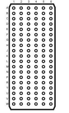
Pinout

  Connection Diagram


Specifications

Storage Temperature . . . . . . . . . . . 65 to +150
Supply Voltage . . . . . . . . . . . . . . . . . . .  -0.5 to 3.6V
Input Voltage1 . . . . . . . . . . . . . .  . -0.5 to VDD +0.5
Output Voltage1,2 . . . . . . . . . . . . -0.5 to VDDQ +0.5
Input Clamp Current . . . . . . . . . . . . . . . . . . ±50 mA
Output Clamp Current . . . . . . . . . . . . . . . . .. ±50mA
Continuous Output Current . . . . . . . . . . . . .  ±50mA
VDD, VDDQ or GND Current/Pin . . . . . . . . . . ±100mA
Package Thermal Impedance3 . . . . . . . . . . . . 55/W
Notes:
1. The input and output negative voltage ratings may be excluded if the input and output clamp ratings are observed.
2. This current will flow only when the output is in the high state level V0 >VDDQ.
3. The package thermal impedance is calculated in accordance with JESD 51.


Description

The 24-bit-to-48-bit ICSSSTV32852 is a universal bus driver designed for 2.3V to 2.7V VDD operation and SSTL_2 I/ O levels, except for the LVCMOS RESET# input.

Data flow from D to Q is controlled by the differential clock (CLK/CLK#) and a control signal (RESET#). The positive edge of CLK is used to trigger the data flow and CLK# is used to maintain sufficient noise margins where as RESET#, an LVCMOS asynchronous signal, is intended for use at the time of power-up only. ICSSSTV32852 supports low-power standby operation. A logic level "Low" at RESET# assures that all internal registers and outputs (Q) are reset to the logic "Low" state, and all input receivers, data (D) and clock (CLK/CLK#) are switched off. Please note that RESET# must always be supported with LVCMOS levels at a valid logic state because VREF may not be stable during powerup.

To ensure that outputs of the ICSSSTV32852 are at a defined logic state before a stable clock has been supplied, RESET# must be held at a logic "Low" level during power up.

 In the DDR DIMM application, RESET# is specified to be completely asynchronous with respect to CLK and CLK#. Therefore, no timing relationship can be guaranteed between the two signals. When entering a low-power standby state, the register will be cleared and the outputs will be driven to a logic "Low" level quickly relative to the time to disable the differential input receivers. This ensures there are no glitches on the output. However, when coming out of low-power standby state, the register will become active quickly relative to the time to enable the differential input receivers. When the data inputs are at a logic level "Low" and the clock is stable during the "Low"-to-"High" transition of RESET# until the input receivers of the ICSSSTV32852 are fully enabled, the design ensures that the outputs will remain at a logic "Low" level.


Customers Who Bought This Item Also Bought

Margin,quality,low-cost products with low minimum orders. Secure your online payments with SeekIC Buyer Protection.
RF and RFID
Soldering, Desoldering, Rework Products
Discrete Semiconductor Products
Transformers
View more