IDT23S08T

Features: • Phase-Lock Loop Clock Distribution for Applications ranging from 10MHz to 133MHz operating frequency• Distributes one clock input to two banks of four outputs• Separate output enable for each output bank• External feedback (FBK) pin is used to synchronize the ou...

product image

IDT23S08T Picture
SeekIC No. : 004371648 Detail

IDT23S08T: Features: • Phase-Lock Loop Clock Distribution for Applications ranging from 10MHz to 133MHz operating frequency• Distributes one clock input to two banks of four outputs• Separate...

floor Price/Ceiling Price

Part Number:
IDT23S08T
Supply Ability:
5000

Price Break

  • Qty
  • 1~5000
  • Unit Price
  • Negotiable
  • Processing time
  • 15 Days
Total Cost: $ 0.00

SeekIC Buyer Protection PLUS - newly updated for 2013!

  • Escrow Protection.
  • Guaranteed refunds.
  • Secure payments.
  • Learn more >>

Month Sales

268 Transactions

Rating

evaluate  (4.8 stars)

Upload time: 2024/5/1

Payment Methods

All payment methods are secure and covered by SeekIC Buyer Protection PLUS.

Notice: When you place an order, your payment is made to SeekIC and not to your seller. SeekIC only pays the seller after confirming you have received your order. We will also never share your payment details with your seller.
Product Details

Description


Features:

• Phase-Lock Loop Clock Distribution for Applications ranging
   from 10MHz to 133MHz operating frequency
• Distributes one clock input to two banks of four outputs
• Separate output enable for each output bank
• External feedback (FBK) pin is used to synchronize the outputs
   to the clock input
• Output Skew <200 ps
• Low jitter <200 ps cycle-to-cycle
• 1/2x, 1x, 2x, 4x output options (see table):
IDT23S08T-1 1x
IDT23S08T-2 1x, 2x
IDT23S08T-3 2x, 4x
IDT23S08T-4 2x
IDT23S08T-5 1/2x
• No external RC network required
• Operates at 2.5V VDD
• Spread spectrum compatible
• Available in SOIC package


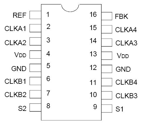
Pinout

  Connection Diagram


Specifications

Parameter Conditions/Description Min. Max. Units
Ambient Temperature Range   -40 85 °C
Storage Temperature (Ts)   -55 150 °C
Junction Temperature (TJ)     125 °C
Input Voltage VDD pin -0.3 3.6 VDC
Input Voltage Any pin other than VDD -0.5 VDD+0.5 VDC
Pin Current DC   40 mA

NOTES:
1. Stresses greater than those listed under ABSOLUTE MAXIMUM RATINGS may
  cause permanent damage to the device. This is a stress rating only and functional
  operation of the device at these or any other conditions above those indicated in the
  operational sections of this specification is not implied. Exposure to absolute maximum
  rating conditions for extended periods may affect reliability.
2. The input and output negative-voltage ratings may be exceeded if the input and output
  clamp-current ratings are observed.
3. The maximum package power dissipation is calculated using a junction temperature
  of 150°C and a board trace length of 750 mils


Symbol Rating Max. Unit
VDD Supply Voltage Range 0.5 to +4.6 v
VI (2) Input Voltage Range (REF) 0.5 to +5.5 v
VI Input Voltage Range
(except REF)
0.5 to VDD+0.5 v
IIK (VI < 0) Input Clamp Current 50 mA
IO
(VO = 0 to VDD)
Continuous Output Curre ±50 mA
VDD or GND Continuous Current ±100 mA
TA = 55°C
(in still air)(3)
Maximum Power Dissipation 0.7 w
TSTG Storage Temperature Ran 65 to +15 °C
Operating
Temperature
Commercial Tempera Range 0 to +70 °C


Description

The IDT23S08T is a high-speed phase-lock loop (PLL) clock multiplier. It is designed to address high-speed clock distribution and multiplication applications. The zero delay is achieved by aligning the phase between the incoming clock and the output clock, operable within the range of 10 to 133MHz.

The IDT23S08T has two banks of four outputs each that are controlled via two select addresses. By proper selection of input addresses, both banks can be put in tri-state mode. In test mode, the PLL is turned off, and the input clock directly drives the outputs for system testing purposes. In the absence of an input clock, the IDT23S08T enters power down. In this mode, the device will draw less than 12A, and the outputs are tri-stated.

The IDT23S08T is available in six unique configurations for both prescaling and multiplication of the Input REF Clock. (See available options table.)

The PLL is closed externally to provide more flexibility by allowing the user to control the delay between the input clock and the outputs. The IDT23S08T is characterized for Commercial operation


Customers Who Bought This Item Also Bought

Margin,quality,low-cost products with low minimum orders. Secure your online payments with SeekIC Buyer Protection.
Isolators
Undefined Category
Test Equipment
View more