Features: ·128K x 36, 256K x 18 memory configurations
·Supports high performance system speed - 200 MHz (3.2 ns Clock-to-Data Access)
· ZBTTM Feature - No dead cycles between write and read cycles
·Internally synchronized output buffer enable eliminates the need to control OE
·Single R/W (READ/WRITE) control pin
·Positive clock-edge triggered address, data, and control signal registers for fully pipelined applications
·4-word burst capability (interleaved or linear)
·Individual byte write (BW1 - BW4) control (May tie active)
·Three chip enables for simple depth expansion
·3.3V power supply (±5%), 3.3V I/O Supply (VDDQ)
·Optional- Boundary Scan JTAG Interface (IEEE 1149.1 compliant)
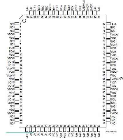
·Packaged in a JEDEC standard 100-pin plastic thin quad flatpack (TQFP), 119 ball grid array (BGA) and 165 fine pitch
ball grid array (fBGA)Pinout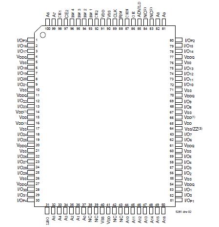
 Specifications
| Symbol |
Rating |
Commercial &
Industrial Values |
Unit |
| VTERM(2) |
Terminal Voltage with
Respect to GND |
-0.5 to +4.6 |
V |
| VTERM(3,6) |
Terminal Voltage with
Respect to GND |
-0.5 to VDD |
V |
| VTERM(4,6) |
Terminal Voltage with
Respect to GND |
-0.5 to VDD +0.5 |
V |
| VTERM(5,6) |
Terminal Voltage with
Respect to GND |
-0.5 to VDDQ +0.5 |
V |
| TA(7) |
Commercial
Operating Temperature |
-0 to +70 |
|
Industrial
Operating Temperature |
-40 to +85 |
|
| TBIAS |
Temperature
Under Bias |
-55 to +125 |
|
| TSTG |
Storage
Temperature |
-55 to +125 |
|
| PT |
Power Dissipation |
2.0 |
W |
| IOUT |
DC Output Current |
50 |
mA |
NOTES:
1. Stresses greater than those listed under ABSOLUTE MAXIMUM RATINGS may cause permanent damage to the device. This is a stress rating only and functional operation of the device at these or any other conditions above those indicated in the operational sections of this specification is not implied. Exposure to absolute maximum ratingconditions for extended periods may affect reliability.
2. VDD terminals only.
3. VDDQ terminals only.
4. Input terminals only.
5. I/O terminals only.
6. This is a steady-state DC parameter that applies after the power supply has reached its nominal operating value. Power sequencing is not necessary; however, the voltage on any input or I/O pin cannot exceed VDDQ during power
supply ramp up.
7. TA is the "instant on" case temperature.DescriptionThe IDT71V3558SA are 3.3V high-speed 4,718,592-bit (4.5 Megabit) synchronous SRAMS. They are designed to eliminate dead bus cycles when turning the bus around between reads and writes, or writes and reads. Thus, they have been given the name ZBTTM, or Zero Bus Turnaround.
Address and control signals are applied to the SRAM during one clock cycle, and two cycles later the associated data cycle occurs, be it read or write.
The IDT71V3558SA contain data I/O, address and control signal registers. Output enable is the only asynchronous signal and can be used to disable the outputs at any given time.
A Clock Enable (CEN) pin allows operation of the IDT71V3558SA to be suspended as long as necessary. All synchronous inputs are ignored when (CEN) is high and the internal device registers will hold their previous values.
There are three chip enable pins (CE1, CE2, CE2) of the IDT71V3558SA that allow the user to deselect the device when desired. If any one of these three are not asserted when ADV/LD is low, no new memory operation can be initiated. However, any pending data transfers (reads or writes) will be completed. The data bus will tri-state two cycles after chip is deselected or a write is initiated.

 IDT71V3558SA Data Sheet