Features: • Choose among the following memory organizations:
IDT72261LA 16,384 x 9
IDT72271LA 32,768 x 9
• Pin-compatible with the IDT72281/72291 SuperSync FIFOs
• 10ns read/write cycle time (8ns access time)
• Fixed, low first word data latency time
• Auto power down minimizes standby power consumption
• Master Reset clears entire FIFO
• Partial Reset clears data, but retains programmable settings
• Retransmit operation with fixed, low first word data latency time
• Empty, Full and Half-Full flags signal FIFO status
• Programmable Almost-Empty and Almost-Full flags, each flag
can default to one of two preselected offsets
• Program partial flags by either serial or parallel means
• Select IDT Standard timing (using EF and FF flags) or First
Word Fall Through timing (using OR and IR flags)
• Output enable puts data outputs into high impedance state
• Easily expandable in depth and width
• Independent Read and Write clocks (permit reading and writing
simultaneously) • Available in the 64-pin Thin Quad Flat Pack (TQFP) and the 64-
pin Slim Thin Quad Flat Pack (STQFP)
• High-performance submicron CMOS technology
• Industrial temperature range (40°C to +85°C) is availablePinout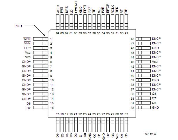 Specifications
|
Symbol |
Rating |
Com'l & Ind'l |
Unit |
|
VTERM |
Terminal Voltage
with respect to GND |
0.5 to +7 |
V |
|
TSTG |
Storage
Temperature |
55 to +125 |
°C |
|
IOUT |
DC Output Current |
50 to +50 |
mA |
NOTE:1. Stresses greater than those listed under ABSOLUTE MAXIMUM RATINGS may cause permanent damage to the device. This is a stress rating only and functional operation of the device at these or any other conditions above those indicated in the operational sections of this specification is not implied. Exposure to absolute maximum rating conditions for extended periods may affect reliability.DescriptionThe IDT72271LA are exceptionally deep, high speed, CMOS First-In-First-Out (FIFO) memories with clocked read and write controls. These FIFOs offer numerous improvements over previous SuperSync FIFOs, including the following:
• The limitation of the frequency of one clock input with respect to the other has been removed. The Frequency Select pin (FS has been removed, thus it is no longer necessary to select which of the two clock inputs,RCLK or WCLK, is running at the higher frequency.
• The period required by the retransmit operation is now fixed and short.
• The first word data latency period, from the time the first word is written to an empty FIFO to the time it can be read, is now fixed and short. (The
variable clock cycle counting delay associated with the latency period found on previous SuperSync devices has been eliminated on this SuperSync
family.)
SuperSync FIFOs of the IDT72271LA are particularly appropriate for network, video, telecommunications, data communications and other applications that need to buffer arge amounts of data.
The input port of the IDT72271LA is controlled by a Write Clock (WCLK) input and a Write Enable,WEN) input. Data is written into the FIFO on every rising edge of WCLK when ,WEN is asserted. The output port is controlled by a Read Clock (RCLK) input and Read Enable (,REN) input. Data is read from the FIFO on every rising edge of RCLK when ,REN is asserted. An Output Enable (,OE) input is provided or three-state control of the outputs.
The frequencies of both the RCLK and the WCLK signals may vary from 0 o fMAX with complete independence. There are no restrictions on the
requency of one clock input with respect to the other.
There are two possible timing modes of operation with these devices: DT Standard mode and First Word Fall Through (FWFT) mode.
In IDT Standard mode of the IDT72271LA, the first word written to an empty FIFO will not appear on the data output lines unless a specific read operation is performed. A read operation, which consists of activating REN and enabling a rising RCLK edge, will shift the word from internal memory to the data outputnes.

 IDT72271LA Data Sheet