SeekIC No. : 004372742
Detail
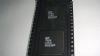
IDT74ALVC244PG: PinoutDescriptionThe IDT74ALVC244PG is built using advanced dual metal CMOS technology.The IDT74ALVC244PG is organized as two 4-bit line drivers with separate output-enable (OE) inputs.When OE is lo...
 IDT74ALVC244PG Data Sheet
floor Price/Ceiling Price
- Part Number:
- IDT74ALVC244PG
- Supply Ability:
- 5000
Price Break
- Qty
- 1~5000
- Unit Price
- Negotiable
- Processing time
- 15 Days
SeekIC Buyer Protection PLUS - newly updated for 2013!
- Escrow Protection.
- Guaranteed refunds.
- Secure payments.
- Learn more >>
Month Sales
268 Transactions
Payment Methods
All payment methods are secure and covered by SeekIC Buyer Protection PLUS.
Notice: When you place an order, your payment is made to SeekIC and not to your seller. SeekIC only pays the seller after confirming you have received your order. We will also never share your payment details with your seller.