IDT74FCT534AT

Features: • A and C grades• Low input and output leakage 1A (max.)• CMOS power levels• True TTL input and output compatibility: VOH = 3.3V (typ.) VOL = 0.3V (typ.)• High Drive outputs (-15mA IOH, 48mA IOL)• Meets or exceeds JEDEC standard 18 specificationsR...

product image

IDT74FCT534AT Picture
SeekIC No. : 004373055 Detail

IDT74FCT534AT: Features: • A and C grades• Low input and output leakage 1A (max.)• CMOS power levels• True TTL input and output compatibility: VOH = 3.3V (typ.) VOL = 0.3V (typ.)• H...

floor Price/Ceiling Price

Part Number:
IDT74FCT534AT
Supply Ability:
5000

Price Break

  • Qty
  • 1~5000
  • Unit Price
  • Negotiable
  • Processing time
  • 15 Days
Total Cost: $ 0.00

SeekIC Buyer Protection PLUS - newly updated for 2013!

  • Escrow Protection.
  • Guaranteed refunds.
  • Secure payments.
  • Learn more >>

Month Sales

268 Transactions

Rating

evaluate  (4.8 stars)

Upload time: 2024/4/28

Payment Methods

All payment methods are secure and covered by SeekIC Buyer Protection PLUS.

Notice: When you place an order, your payment is made to SeekIC and not to your seller. SeekIC only pays the seller after confirming you have received your order. We will also never share your payment details with your seller.
Product Details

Description


Features:

• A and C grades
• Low input and output leakage 1A (max.)
• CMOS power levels
• True TTL input and output compatibility: VOH = 3.3V (typ.) VOL = 0.3V (typ.)
• High Drive outputs (-15mA IOH, 48mA IOL)
• Meets or exceeds JEDEC standard 18 specifications
• Power off disable outputs permit "live insertion"
• Available in SOIC and QSOP packages


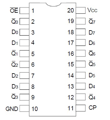
Pinout

  Connection Diagram


Specifications

Symbol

Description
Max
Unit
VTERM(2)
Terminal Voltage with Respect to GND
0.5 to +7
V
VTERM(3)
Terminal Voltage with Respect to GND
0.5 to VCC+0.5
V
TSTG
Storage Temperature
65 to +150
°C

IOUT

DC Output Current
60 to +120
mA

NOTES:
1. Stresses greater than those listed under ABSOLUTE MAXIMUM RATINGS may cause permanent damage to the device. This is a stress rating only and functional operation of the device at these or any other conditions above those indicated in the operational sections of this specification is not implied. Exposure to absolute maximum rating conditions for extended periods may affect reliability. No terminal voltage may exceed Vcc by +0.5V unless otherwise noted.
2. Inputs and Vcc terminals only.
3. Output and I/O terminals only.


Description

The IDT74FCT534AT is an 8-bit register built using an advanced dual metal CMOS technology. These registers consist of eight D-type flip-flops with a buffered common clock and buffered 3-state output control. When the output enable (OE) input is low, the eight outputs are enabled. When the OE input of the IDT74FCT534AT is high, the outputs are in the high-impedance state. Input data meeting the set-up and hold time requirements of the D inputs is transferred to the Q outputs on the low-to-high transition of the clock input.


Customers Who Bought This Item Also Bought

Margin,quality,low-cost products with low minimum orders. Secure your online payments with SeekIC Buyer Protection.
Motors, Solenoids, Driver Boards/Modules
Prototyping Products
DE1
Memory Cards, Modules
Undefined Category
View more