IDT74SSTV16859

Features: •2.3V to 2.7V Operation• SSTL_2 Class II style data inputs/outputs• Differential CLK input• RESET control compatible with LVCMOS levels• Latch-up performance exceeds 100mA• ESD >2000V per MIL-STD-883, Method 3015; >200V using machine model (C = 2...

product image

IDT74SSTV16859 Picture
SeekIC No. : 004373248 Detail

IDT74SSTV16859: Features: •2.3V to 2.7V Operation• SSTL_2 Class II style data inputs/outputs• Differential CLK input• RESET control compatible with LVCMOS levels• Latch-up performance ...

floor Price/Ceiling Price

Part Number:
IDT74SSTV16859
Supply Ability:
5000

Price Break

  • Qty
  • 1~5000
  • Unit Price
  • Negotiable
  • Processing time
  • 15 Days
Total Cost: $ 0.00

SeekIC Buyer Protection PLUS - newly updated for 2013!

  • Escrow Protection.
  • Guaranteed refunds.
  • Secure payments.
  • Learn more >>

Month Sales

268 Transactions

Rating

evaluate  (4.8 stars)

Upload time: 2024/4/26

Payment Methods

All payment methods are secure and covered by SeekIC Buyer Protection PLUS.

Notice: When you place an order, your payment is made to SeekIC and not to your seller. SeekIC only pays the seller after confirming you have received your order. We will also never share your payment details with your seller.
Product Details

Description


Features:

•2.3V to 2.7V Operation
• SSTL_2 Class II style data inputs/outputs
• Differential CLK input
• RESET control compatible with LVCMOS levels
• Latch-up performance exceeds 100mA
• ESD >2000V per MIL-STD-883, Method 3015; >200V using machine model (C = 200pF, R = 0)
• Available in 56 pin MLF and 64 pin TSSOP packages


Application

• Ideally suited for DIMM DDR registered applications


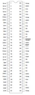
Pinout

  Connection Diagram


Specifications

Symbol
Description
Max
Unit
VDD or VDDQ
Supply Voltage Range
0.5 to 3.6
V
VI(2)
Input Voltage Range
0.5 to VDD +0.5
V
VO(3)
Output Voltage Range
0.5 to VDDQ +0.5
V
IIK
Input Clamp Current, VI < 0
50
mA
IOK
Output Clamp Current,
VO < 0 or VO > VDDQ
±50
mA
IO
Continuous Output Current,
VO = 0 to VDDQ
±50
mA
VDD
Continuous Current through each
VDD, VDDQ or GND
±100
mA
TSTG
Storage Temperature Range.
65 to +150
°C

NOTES:
1. Stresses greater than those listed under ABSOLUTE MAXIMUM RATINGS may cause permanent damage to the device. This is a stress rating only and functional operation of the device at these or any other conditions above those indicated in the operational sections of this specification is not implied. Exposure to absolute maximum rating conditions for extended periods may affect reliability.
2. The input and output negative voltage ratings may be exceeded if the ratings of the I/P and O/P clamp current are observed.
3. The output current will flow if the following conditions are observed: a) Output in HIGH state b) VO = VDDQ


Description

The IDT74SSTV16859 is a 13-bit to 26-bit registered buffer designed for 2.3V- 2.7V VDD and supports low standby operation. All data inputs and outputs are SSTL_2 level compatible with JEDEC standard for SSTL_2.

RESETis an LVCMOS input since it must operate predictably during the power-up phase. RESET, which can be operated independent of CLK and CLK, must be held in the low state during power-up in order to ensure predictable outputs (low state) before a stable clock has been applied.

RESET, when in the low state, will disable all input receivers, reset all registers of the IDT74SSTV16859, and force all outputs to a low state, before a stable clock has been applied. With inputs held low and a stable clock applied, outputs will remain  low during the Low-to-High transition of RESET.


Customers Who Bought This Item Also Bought

Margin,quality,low-cost products with low minimum orders. Secure your online payments with SeekIC Buyer Protection.
Integrated Circuits (ICs)
Test Equipment
Circuit Protection
Resistors
Static Control, ESD, Clean Room Products
View more