IDTCSPT855

Features: • PLL clock driver for DDR (Double Data Rate) synchronous DRAM applications• Spread spectrum clock compatible• Operating frequency: 60MHz to 180MHz• Low jitter (cycle-to-cycle): ±50ps• Distributes one differential clock input to four differential clock outpu...

product image

IDTCSPT855 Picture
SeekIC No. : 004373379 Detail

IDTCSPT855: Features: • PLL clock driver for DDR (Double Data Rate) synchronous DRAM applications• Spread spectrum clock compatible• Operating frequency: 60MHz to 180MHz• Low jitter (cyc...

floor Price/Ceiling Price

Part Number:
IDTCSPT855
Supply Ability:
5000

Price Break

  • Qty
  • 1~5000
  • Unit Price
  • Negotiable
  • Processing time
  • 15 Days
Total Cost: $ 0.00

SeekIC Buyer Protection PLUS - newly updated for 2013!

  • Escrow Protection.
  • Guaranteed refunds.
  • Secure payments.
  • Learn more >>

Month Sales

268 Transactions

Rating

evaluate  (4.8 stars)

Upload time: 2024/5/1

Payment Methods

All payment methods are secure and covered by SeekIC Buyer Protection PLUS.

Notice: When you place an order, your payment is made to SeekIC and not to your seller. SeekIC only pays the seller after confirming you have received your order. We will also never share your payment details with your seller.
Product Details

Description


Features:

• PLL clock driver for DDR (Double Data Rate) synchronous DRAM applications
• Spread spectrum clock compatible
• Operating frequency: 60MHz to 180MHz
• Low jitter (cycle-to-cycle): ±50ps
• Distributes one differential clock input to four differential clock outputs
• Enters low power mode and 3-state outputs when input CLK signal is less than 20MHz or PWRDWN is low
• Operates from dual 2.5V supplies
• Consumes <200µA quiescent current
• External feedback pins (FBIN, FBIN) are used to synchronize outputs to input clocks
• Available in TSSOP package


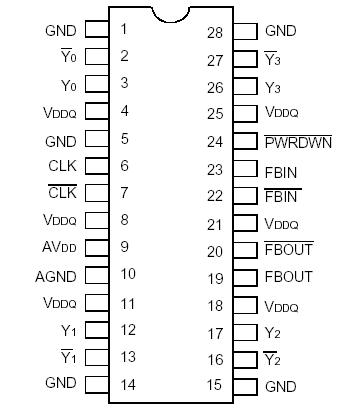
Pinout

  Connection Diagram


Specifications

Rating
Symbol
Max
unit
Supply Voltage Range
V CC1, VCC2
0.5 to +4.6
V
Input Voltage Range
VI (2)
0.5 to +5.5
V
Voltage range applied to any
output in the high or low state
VO(2)
0.5 to VDD + 0.5
V
Input clamp current
IIK (VI < 0)
50
mA
Terminal Voltage with Respect
to GND (inputs VIH 2.5, VIL 2.5)
IOK
(VO < 0 or VO > VDD)
-50
mA
Continuous Output Current
IRES
±100
mA
Continuous Current
VDD or GND
65 to +150
mA
Junction Temperature
TSTG
+150
°C

NOTES:
1. Stresses greater than those listed under ABSOLUTE MAXIMUM RATINGS may cause
permanent damage to the device. This is a stress rating only and functional operation
of the device at these or any other conditions above those indicated in the operational
sections of this specification is not implied. Exposure to absolute maximum rating
conditions for extended periods may affect reliability.
2. The input and output negative-voltage ratings may be exceeded if the input and output
clamp-current ratings are observed. This value is limited to 3.6V maximum.
3. The package thermal impedance is calculated in accordance with JESD 51.


Description

The CSPT855 is a high-performance, low-skew, low-jitter zero delay buffer that distributes one differential clock input pair(CLK, CLK ) to four differential output pairs (Y [0:3], Y [0:3]) and one differential pair of feedback clock outputs FBOUT, FBOUT). When PWRDWN IDTCSPT855 is high, the outputs switch in phase and frequency with CLK. When PWRDWN is low, all outputs of IDTCSPT855 are disabled to a highimpedance state (3-state), and the PLL is shut down (low-power mode).

IDTCSPT855 also enters this low-power mode when the input frequency falls below suggested detection frequency that is below 20MHz (typical 10MHz). An input frequency detection circuit detects the low-frequency condition, and after applying a >20MHz input signal, this detection circuit reactivates the PLL and enables the outputs. When AVDD IDTCSPT855 is tied to GND, the PLL is turned off and bypassed for test purposes.

The CSPT855 is also able to track spread spectrum clocking reducted EMI. Since the CSPT855 is based on PLL circuitry, it requires a stabilization time to achieve phase-lock of the PLL. This stabilization time is required following power up.


Customers Who Bought This Item Also Bought

Margin,quality,low-cost products with low minimum orders. Secure your online payments with SeekIC Buyer Protection.
Transformers
LED Products
RF and RFID
Undefined Category
Audio Products
Hardware, Fasteners, Accessories
View more