Features: •Optimized for clock distribution in DDR (Double Data Rate)SDRAM applications
•Operating frequency: 60MHz to 200MHz
•Standard speed: PC1600 (DDR200), PC2100 (DDR266)
•A speed: PC1600 (DDR200), PC2100 (DDR266), PC2700 (DDR333)
•1 to 10 differential clock distribution
•Very low skew (<100ps)
•Very low jitter (<75ps)
•2.5V AVDD and 2.5V VDDQ
•CMOS control signal input
•Test mode enables buffers while disabling PLL
•Low current power-down mode
•Tolerant of Spread Spectrum input clock
•Available in 48-pin TSSOP and 56-pin VFBGA packagesPinout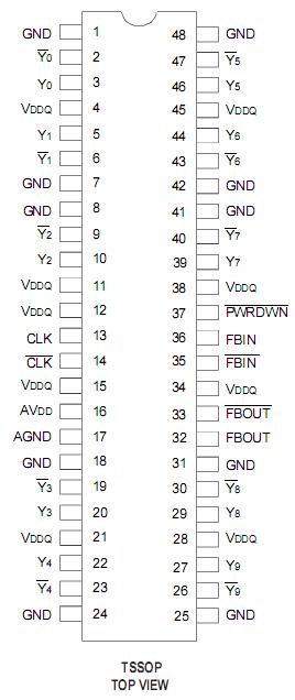 Specifications
| Symbol |
Rating |
Max |
Unit |
| VDDQ, AVDD |
Supply Voltage Range |
0.5 to +3.6 |
V |
| VI(2) |
Input Voltage Range |
0.5 to VDDQ+0.5 |
V |
| VO(2) |
Voltage range applied to any
output in the high or low state |
0.5 to VDDQ+0.5 |
V |
IIK
(VI <0) |
Input Clamp Current |
50 |
mA |
IOK
(VO <0 or
VO > VDDQ) |
Output Clamp Current |
±50 |
mA |
IO
(VO =0 to VDDQ) |
Continuous Output Current |
±50 |
mA |
| VDDQ or GND |
Continuous Current |
±100 |
mA |
| TSTG |
Storage Temperature Range |
65 to +150 |
°C |
DescriptionThe CSPT857 is a PLL based clock driver that acts as a zero delay buffer to distribute one differential clock input pair(CLK, CLK</a> ) to 10 differential output
pairs (Y[0:9],Y [0:9]</a>) and one differential pair of feedback clock output (FBOUT,FBOUT</a>). External feedback pins (FBIN, FBIN</a>)IDTCSPT857/A for synchronization of the outputs to the input reference is provided. A CMOS Enable/Disable pin of IDTCSPT857/A is available for low power disable. When the output frequency falls below approximately 20MHz, the device will enter power down mode. In this mode of IDTCSPT857/A, the receivers are disabled, the PLL is turned off, and the output clock drivers are tristated, resulting in a current consumption device of less than 200µA.
The CSPT857 requires no external components and has been optimised for very low I/O phase error, skew, and jitter, while maintaining frequency and duty cycle over the operating voltage and temperature range. The CSPT857, designed for use in both module assemblies and system motherboard based solutions, provides an optimum high-performance clock source.
The CSPT857 is only available in Industrial Temperature Range (-40°C to+85°C), and CSPT857A is only available in Commercial Temperature Range(0°C to +70°C). See Ordering Information for details.

 IDTCSPT857/A Data Sheet


