IDTQS3VH251

Features: • N channel FET switches with no parasitic diode to VCC Isolation under power-off conditions No DC path to VCC or GND 5V tolerant in OFF and ON state• 5V tolerant I/Os• Low RON - 4 typical• Flat RON characteristics over operating range• Rail-to-rail switc...

product image

IDTQS3VH251 Picture
SeekIC No. : 004373480 Detail

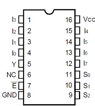
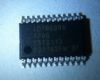
IDTQS3VH251: Features: • N channel FET switches with no parasitic diode to VCC Isolation under power-off conditions No DC path to VCC or GND 5V tolerant in OFF and ON state• 5V tolerant I/Os•...
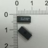
floor Price/Ceiling Price

Part Number:
IDTQS3VH251
Supply Ability:
5000

Price Break

  • Qty
  • 1~5000
  • Unit Price
  • Negotiable
  • Processing time
  • 15 Days
Total Cost: $ 0.00

SeekIC Buyer Protection PLUS - newly updated for 2013!

  • Escrow Protection.
  • Guaranteed refunds.
  • Secure payments.
  • Learn more >>

Month Sales

268 Transactions

Rating

evaluate  (4.8 stars)

Upload time: 2024/5/5

Payment Methods

All payment methods are secure and covered by SeekIC Buyer Protection PLUS.

Notice: When you place an order, your payment is made to SeekIC and not to your seller. SeekIC only pays the seller after confirming you have received your order. We will also never share your payment details with your seller.
Product Details

Description


Features:

• N channel FET switches with no parasitic diode to VCC
   Isolation under power-off conditions
   No DC path to VCC or GND
   5V tolerant in OFF and ON state
• 5V tolerant I/Os
• Low RON - 4 typical
• Flat RON characteristics over operating range
• Rail-to-rail switching 0 - 5V
• Bidirectional dataflow with near-zero delay: no added ground bounce
• Excellent RON matching between channels
• VCC operation: 2.3V to 3.6V
• High bandwidth - up to 500MHz
• LVTTL-compatible control Inputs
• Undershoot Clamp Diodes on all switch and control Inputs
• Low Demux capacitance, 4pF typical
• Available in QSOP and TSSOP packages


Application

• Hot-swapping
• Multiplexing/demultiplexing
• Low distortion analog switch
• Replaces mechanical relay
• ATM 25/155 switching


Pinout

  Connection Diagram


Specifications

Symbol
Description
Max
Unit
VTERM(2)
Supply Voltage to Ground
0.5 to 4.6
V
VTERM(3)
DC Switch Voltage VS
0.5 to 5.5
V
VTERM(3)
DC Input Voltage VIN
0.5 to 5.5
V
VAC
AC Input Voltage (pulse width 20ns)
3
V
IOUT
DC Output Current (max. current/pin)
120
mA
TSTG
Storage Temperature
65 to +15
°C

NOTES:
1. Stresses greater than those listed under ABSOLUTE MAXIMUM RATINGS may cause permanent damage to the device. This is a stress rating only and functional operation of the device at these or any other conditions above those indicated in the operational sections of this specification is not implied. Exposure to absolute maximum rating conditions for extended periods may affect reliability.
2. VCC terminals.
3. All terminals except VCC.


Description

The IDTQS3VH251 HotSwitch Quad 2:1 multiplexer/demultiplexer is a high bandwidth bus switch. The IDTQS3VH251 has very low ON resistance, resulting in under 250ps propagation delay through the switch. The Select (Sx) input controls the data flow. The multiplexers/demultiplexers are enabled when the Enable (E) input is low. In the ON state, the switches can pass signals up to 5V. In the OFF state, the switches offer very high impedence at the terminals.

The combination of near-zero propagation delay, high OFF impedance, and over-voltage tolerance makes the IDTQS3VH251 ideal for high performance comminucation applications.

The IDTQS3VH251 is characterized for operation from -40°C to +85°C.


Customers Who Bought This Item Also Bought

Margin,quality,low-cost products with low minimum orders. Secure your online payments with SeekIC Buyer Protection.
Prototyping Products
DE1
Resistors
Potentiometers, Variable Resistors
View more