Features: • Clock frequency: 143 MHz• Fully synchronous; all signals referenced to a positive clock edge• Internal bank for hiding row access/precharge• Single 3.3V power supply• LVTTL interface• Programmable burst length: (1, 2, 4, 8, full page)• Programm...
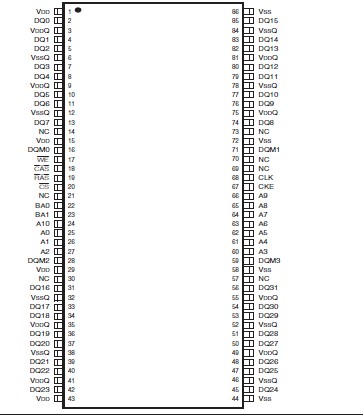
IS45S32200C1: Features: • Clock frequency: 143 MHz• Fully synchronous; all signals referenced to a positive clock edge• Internal bank for hiding row access/precharge• Single 3.3V power sup...
SeekIC Buyer Protection PLUS - newly updated for 2013!
268 Transactions
All payment methods are secure and covered by SeekIC Buyer Protection PLUS.

|
Symbol |
Parameters |
Rating |
Unit |
|
V DD MAX V DDQ M AX VIN VOUT P D MAX ICS TOPR TSTG |
Maximum Supply Voltage Maximum Supply Voltage for Output Buffer Input Voltage Output Voltage Allowable Power Dissipation Output Shorted Current Operating Temperature A: A1: Storage Temperature |
1.0 to +4.6 1.0 to +4.6 1.0 to +4.6 1.0 to +4.6 1 50 0 to +70 -40 to +85 55 to +150 |
V V V V W mA °C °C °C |
Notes:
1. Stress greater than those listed under ABSOLUTE MAXIMUM RATINGS may cause permanent damage to the device. This is a stress rating only and functional operation of the device at these or any other conditions above those indicated in the operational sections of this specification is not implied. Exposure to absolute maximum rating conditions for extended periods may affect reliability.
2. All voltages are referenced to GND.
3. VIH (max) = VDDQ + 2.0V with a pulse width 3 ns. The pluse width cannot be greater than one third of the cycle rate.
4. VIL (min) = GND 2.0V with a pulse < 3 ns. The pluse width cannot be greater than one third of the cycle rate.
5. An initial pause of 100us is required after power up, followed by two AUTO REFRESH commands, before proper device operation is ensured. (Vdd and VddQ must be powered up simultaneously. GND and GNDQ must be at same potential.) The two AUTO REFRESH command wake-ups should be repeated anytime the tREF refresh requirement is exceeded.
ISSI's 64Mb Synchronous DRAM IS45S32200C1 is organized as 524,288 bits x 32-bit x 4-bank for improved performance. The synchronous DRAMs achieve highspeed data transfer using pipeline architecture. All inputs and outputs signals refer to the rising edge of the clock input.