IS45S32400B

Features: • Clock frequency: 166, 143, 125, 100 MHz• Fully synchronous; all signals referenced to a positive clock edge• Internal bank for hiding row access/precharge• Power supply VDD VDDQ IS45S32400B 3.3V 3.3V• LVTTL interface• Programmable burst length (1, 2,...

product image

IS45S32400B Picture
SeekIC No. : 004379077 Detail

IS45S32400B: Features: • Clock frequency: 166, 143, 125, 100 MHz• Fully synchronous; all signals referenced to a positive clock edge• Internal bank for hiding row access/precharge• Power ...

floor Price/Ceiling Price

Part Number:
IS45S32400B
Supply Ability:
5000

Price Break

  • Qty
  • 1~5000
  • Unit Price
  • Negotiable
  • Processing time
  • 15 Days
Total Cost: $ 0.00

SeekIC Buyer Protection PLUS - newly updated for 2013!

  • Escrow Protection.
  • Guaranteed refunds.
  • Secure payments.
  • Learn more >>

Month Sales

268 Transactions

Rating

evaluate  (4.8 stars)

Upload time: 2024/5/3

Payment Methods

All payment methods are secure and covered by SeekIC Buyer Protection PLUS.

Notice: When you place an order, your payment is made to SeekIC and not to your seller. SeekIC only pays the seller after confirming you have received your order. We will also never share your payment details with your seller.
Product Details

Description


Features:

• Clock frequency: 166, 143, 125, 100 MHz
• Fully synchronous; all signals referenced to a positive clock edge
• Internal bank for hiding row access/precharge
• Power supply VDD VDDQ IS45S32400B 3.3V 3.3V
• LVTTL interface
• Programmable burst length
(1, 2, 4, 8, full page)
• Programmable burst sequence:Sequential/Interleave
• Auto Refresh (CBR)
• Self Refresh with programmable refresh periods
• 4096 refresh cycles every 64 ms
• Random column address every clock cycle
• Programmable CAS latency (2, 3 clocks)
• Burst read/write and burst read/single write operations capability
• Burst termination by burst stop and precharge command
• Automotive Temperature Range Option A: 0 to +70  Option A1: -40 to +85
• Available in 86-pin TSOP-II and 90-ball FBGA
• Available in Lead-free


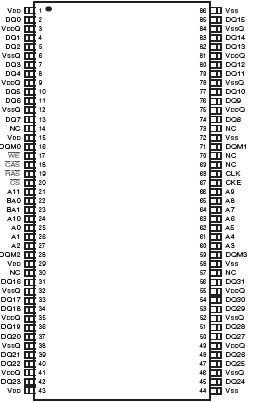
Pinout

  Connection Diagram


Specifications

Symbol Parameters
Rating
Unit
VDD MAX Maximum Supply Voltage
0.5 to +4.6
V
VDDQ
MAX
Maximum Supply Voltage for Output Buffer
0.5 to +4.6
V
VIN Input Voltage
0.5 to V + 0.5
V
VOUT Output Voltage
1.0 to VDDQ + 0.5
V
PD MAX Allowable Power Dissipation
1
W
ICS Output Shorted Current
50
mA
TOPR Operating Temperature
A 0 to +70
A1 40 to +85
TSTG Storage Temperature
65 to +150
1. Stress greater than those listed under ABSOLUTE MAXIMUM RATINGS may cause permanent damage to the device. This is a stress rating only and functional operation of the device at these or any other conditions above those indicated in the operational sections of this specification is not implied. Exposure to absolute maximum rating conditions for extended periods may affect reliability.
2. All voltages are referenced to Vss.


Customers Who Bought This Item Also Bought

Margin,quality,low-cost products with low minimum orders. Secure your online payments with SeekIC Buyer Protection.
Discrete Semiconductor Products
Audio Products
Soldering, Desoldering, Rework Products
Boxes, Enclosures, Racks
Optical Inspection Equipment
Line Protection, Backups
View more