K4C5608/1638C

Features: • Fully Synchronous Operation Double Data Rate (DDR) Data input/output are synchronized with both edges of DQS. Differential Clock (CK and CK)inputs CS, FN and all address input signals are sampled on the positive edge of CK. Output data (DQs and DQS) is referenced to the crossings...

product image

K4C5608/1638C Picture
SeekIC No. : 004382677 Detail

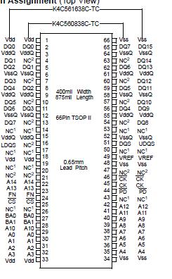
K4C5608/1638C: Features: • Fully Synchronous Operation Double Data Rate (DDR) Data input/output are synchronized with both edges of DQS. Differential Clock (CK and CK)inputs CS, FN and all address input sign...

floor Price/Ceiling Price

Part Number:
K4C5608/1638C
Supply Ability:
5000

Price Break

  • Qty
  • 1~5000
  • Unit Price
  • Negotiable
  • Processing time
  • 15 Days
Total Cost: $ 0.00

SeekIC Buyer Protection PLUS - newly updated for 2013!

  • Escrow Protection.
  • Guaranteed refunds.
  • Secure payments.
  • Learn more >>

Month Sales

268 Transactions

Rating

evaluate  (4.8 stars)

Upload time: 2024/4/26

Payment Methods

All payment methods are secure and covered by SeekIC Buyer Protection PLUS.

Notice: When you place an order, your payment is made to SeekIC and not to your seller. SeekIC only pays the seller after confirming you have received your order. We will also never share your payment details with your seller.
Product Details

Description


Features:

• Fully Synchronous Operation
    Double Data Rate (DDR)
    Data input/output are synchronized with both edges of DQS.
    Differential Clock (CK and CK)inputs
    CS, FN and all address input signals are sampled on the positive edge of CK.
    Output data (DQs and DQS) is referenced to the crossings of CK and CK.
• Fast clock cycle time of 5ns minimum Clock : 200MHz maximum
                                                             Data : 400Mbps/pin maximum
• Quad independent banks operation
• Fast cycle and short Iatency
• Bidirectional data strobe signal
• Distributed Auto-Refresh cycle in 7.8us
• Self-Refresh
• Power Down Mode
• Variable Write Length Control
• Write Latency = CAS Latency - 1
• Programmable CAS Latency and Burst Length
    CAS Latency = 3, 4
    Burst Length = 2, 4
• Organization K4C561638C-TC : 4,194,304 words x4 banks x 16
                        K4C560838C-TC : 8,388,608 words x4 banks x 8
• Power supply voltage Vdd : 2.5 ± 0.15V
                                      VddQ : 2.5 ± 0.15V
• 2.5V CMOS I/O comply with SSTL-2 (Strong / Normal / Weaker / Weakest)
• Package 400X875mil, 66pin TSOP II, 0.65mm pin pitch (TSOP II 66-P-400-0.65)


Pinout

  Connection Diagram


Specifications

Symbol Parameter Rating Units Notes
Vdd Power Supply Voltage -0.3 to 3.3 V  
VddQ Power Supply Voltage (for I/O buffer) -0.3 to Vdd + 0.3 V  
VIN Input Voltage -0.3 to Vdd + 0.3 V  
VOUT DQ pin Voltage -0.3 to VddQ + 0.3 V  
VREF Input Reference Voltage -0.3 to Vdd + 0.3 V  
TOPR Operating Temperature 0 to 70  
TSTG Storage Temperature -55 to 150  
TSOLDER Soldering Temperature(10s) 260  
PD Power Dissipation 1 W  
IOUT Short Circuit Output Current ± 50 mA  

Caution : Conditions outside the limits listed under "ABSOLUTE MAXIMUM RATINGS" may cause permanent damage to the device. The device is not meant to be operated under conditions outside the limits described in the operational section of this specification. Exposure to "ABSOLUTE MAXIMUM RATINGS" conditions for extended periods may affect device reliability.


Customers Who Bought This Item Also Bought

Margin,quality,low-cost products with low minimum orders. Secure your online payments with SeekIC Buyer Protection.
Fans, Thermal Management
Power Supplies - External/Internal (Off-Board)
Soldering, Desoldering, Rework Products
Inductors, Coils, Chokes
Hardware, Fasteners, Accessories
Circuit Protection
View more