Features: • JEDEC standard 1.8V ± 0.1V Power Supply
• VDDQ = 1.8V ± 0.1V
• 200 MHz fCK for 400Mb/sec/pin, 267MHz fCK for 533Mb/sec/pin, 333MHz fCK for 667Mb/sec/pin, 400MHz fCK for 800Mb/sec/pin
• 4 Banks
• Posted CAS
• Programmable CAS Latency: 3, 4, 5
• Programmable Additive Latency: 0, 1 , 2 , 3 and 4
• Write Latency(WL) = Read Latency(RL) -1
• Burst Length: 4 , 8(Interleave/nibble sequential)
• Programmable Sequential / Interleave Burst Mode
• Bi-directional Differential Data-Strobe (Single-ended datastrobe is an optional feature)
• Off-Chip Driver(OCD) Impedance Adjustment
• On Die Termination
• Special Function Support
-PASR(Partial Array Self Refresh)
-50ohm ODT
-High Temperature Self-Refresh rate enable
• Average Refresh Period 7.8us at lower than TCASE 85°C,3.9us at 85°C < TCASE < 95 °C
• All of Lead-free products are compliant for RoHS
Specifications
| Symbol |
Parameter |
Rating |
Units |
Notes |
| VDD |
Voltage on VDD pin relative to VSS |
- 1.0 V ~ 2.3V |
V |
1 |
| VDDQ |
Voltage on VDDQ pin relative to VSS |
- 0.5 V ~ 2.3 V |
V |
1 |
| VDDL |
Voltage on VDDL pin relative to VSS |
- 0.5 V ~ 2.3 V |
V |
1 |
| VIN, VOUT |
Voltage on any pin relative to VSS |
- 0.5 V ~ 2.3 V |
V |
1 |
| TSTG |
Storage Temperature |
-55 to +100 |
°C |
1, 2 |
Note :
1. Stresses greater than those listed under "Absolute Maximum Ratings" may cause permanent damage to the device. This is a stress rating only and functional operation of the device at these or any other conditions above those indicated in the operational sections of this specification is not implied.Exposure to absolute maximum rating conditions for extended periods may affect reliability.
2. Storage Temperature is the case surface temperature on the center/top side of the DRAM. For the measurement conditions, please refer to JESD51-2 standard.
DescriptionThe 512Mb DDR2 SDRAM K4T51043QC-ZC(L)D5 is organized as a 32Mbit x 4 I/Os x 4 banks, 16Mbit x 8 I/Os x 4banks or 8Mbit x 16 I/Os x 4 banks device. This synchronous device K4T51043QC-ZC(L)D5 achieves high speed doubledata-rate transfer rates of up to 800Mb/sec/pin (DDR2-800) for general applications.
The chip K4T51043QC-ZC(L)D5 is designed to comply with the following key DDR2 SDRAM features such as posted CAS with additive latency, write latency = read latency -1, Off-Chip Driver(OCD) impedance adjustment and On Die Termination.
All of the control and address inputs are synchronized with a pair of externally supplied differential clocks. Inputs are latched at the crosspoint of differential clocks (CK rising and CK falling). All I/Os are synchronized with a pair of bidirectional strobes (DQS and DQS) in a source synchronous fashion. The address bus is used to convey row, column, and bank address information in a RAS/CAS multiplexing style. For example, 512Mb(x4) device receive 14/11/2 addressing.
The 512Mb DDR2 device K4T51043QC-ZC(L)D5 operates with a single 1.8V ± 0.1V power supply and 1.8V ± 0.1V VDDQ.
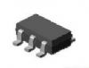
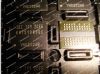
The 512Mb DDR2 device K4T51043QC-ZC(L)D5 is available in 60ball FBGAs(x4/x8) and in 84ball FBGAs(x16).

 K4T51043QC-ZC(L)D5 Data Sheet