Features: • Synchronous Operation.
• 2 Stage Pipelined operation with 4 Burst.
• On-Chip Address Counter.
• Self-Timed Write Cycle.
• On-Chip Address and Control Registers.
• 3.3V+0.165V/-0.165V Power Supply.
• I/O Supply Voltage 3.3V+0.165V/-0.165V for 3.3V I/O or 2.5V+0.4V/-0.125V for 2.5V I/O
• 5V Tolerant Inputs Except I/O Pins.
• Byte Writable Function.
• Global Write Enable Controls a full bus-width write.
• Power Down State via ZZ Signal.
• LBO Pin allows a choice of either a interleaved burst or a linear burst.
• Three Chip Enables for simple depth expansion with No Data Contention only for TQFP ; 2cycle Enable, 1cycle Disable.
• Asynchronous Output Enable Control.
•ADSP, ADSC, ADV Burst Control Pins.
• TTL-Level Three-State Output.
• 100-TQFP-1420A
• Operating in commeical and industrial temperature range.
Pinout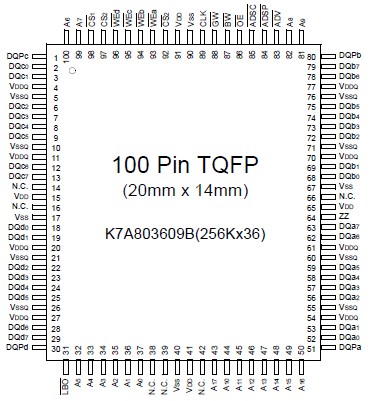 Specifications
| PARAMETER |
SYMBOL |
RATING |
UNIT |
| Voltage on VDD Supply Relative to VSS |
VDD |
-0.3 to 4.6 |
V |
| Voltage on VDDQ Supply Relative to VSS |
VDDQ |
VDD |
V |
| Voltage on Input Pin Relative to VSS |
VIN |
-0.3 to VDD+0.3 |
V |
| Voltage on I/O Pin Relative to VSS |
VIO |
-0.3 to VDDQ+0.3 |
V |
| Power Dissipation |
PD |
2.2 |
W |
| Storage Temperature |
TSTG |
-65 to 150 |
°C |
| Operating Temperature |
Commercial |
TOPR |
0 to 70 |
°C |
| Industrial |
-40 to 85 |
| Storage Temperature Range Under Bias |
TBIAS |
-10 to 85 |
°C |
*Note : Stresses greater than those listed under "Absolute Maximum Ratings" may cause permanent damage to the device. This is a stress rating only and functional operation of the device at these or any other conditions above those indicated in the operating sections of this specification is not implied. Exposure to absolute maximum rating conditions for extended periods may affect reliability.
DescriptionThe K7A803609B and K7A801809B are 9,437,184-bit Synchronous Static Random Access Memory designed for high performance second level cache of Pentium and Power PC based System.
The K7A803609B is organized as 256K(512K) words of 36(18) bits and integrates address and control registers, a 2-bit burst address counter and added some new functions for high performance cache RAM applications; GW, BW, LBO, ZZ. Write cycles are internally self-timed and synchronous.
Full bus-width write is done by GW, and each byte write is performed by the combination of WEx and BW when GW is high. And with CS1 high,ADSP is blocked to control signals.
Burst cycle can be initiated with either the address status processor(ADSP) or address status cache controller(ADSC)inputs. Subsequent burst addresses are generated internally in the systems burst sequence and are controlled by the burst address advance(ADV) input.
LBO pin is DC operated and determines burst sequence(linear or interleaved).
ZZ pin controls Power Down State and reduces Stand-by current regardless of CLK.
The K7A803609B and K7A801809B are fabricated using SAMSUNGs high performance CMOS technology and is available in a 100pin TQFP and Multiple power and ground pins are utilized to minimize ground bounce.

 K7A803609B Data Sheet