K7N163645M

Features: • 2.5V ±5% Power Supply.• Byte Writable Function.• Enable clock and suspend operation.• Single READ/WRITE control pin.• Self-Timed Write Cycle.• Three Chip Enable for simple depth expansion with no data contention .• A interleaved burst or a line...

product image

K7N163645M Picture
SeekIC No. : 004383310 Detail

K7N163645M: Features: • 2.5V ±5% Power Supply.• Byte Writable Function.• Enable clock and suspend operation.• Single READ/WRITE control pin.• Self-Timed Write Cycle.• Three C...

floor Price/Ceiling Price

Part Number:
K7N163645M
Supply Ability:
5000

Price Break

  • Qty
  • 1~5000
  • Unit Price
  • Negotiable
  • Processing time
  • 15 Days
Total Cost: $ 0.00

SeekIC Buyer Protection PLUS - newly updated for 2013!

  • Escrow Protection.
  • Guaranteed refunds.
  • Secure payments.
  • Learn more >>

Month Sales

268 Transactions

Rating

evaluate  (4.8 stars)

Upload time: 2024/3/28

Payment Methods

All payment methods are secure and covered by SeekIC Buyer Protection PLUS.

Notice: When you place an order, your payment is made to SeekIC and not to your seller. SeekIC only pays the seller after confirming you have received your order. We will also never share your payment details with your seller.
Product Details

Description


Features:

• 2.5V ±5% Power Supply.
• Byte Writable Function.
• Enable clock and suspend operation.
• Single READ/WRITE control pin.
• Self-Timed Write Cycle.
• Three Chip Enable for simple depth expansion with no data contention .
• A interleaved burst or a linear burst mode.
• Asynchronous output enable control.
• Power Down mode.
• TTL-Level Three-State Outputs.
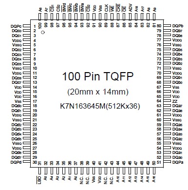
• 100-TQFP-1420A / 119BGA(7x17 Ball Grid Array Package).


Pinout

  Connection Diagram


Specifications

PARAMETER SYMBOL RATING UNIT
Voltage on VDD Supply Relative to VSS VDD -0.3 to 3.6 V
Voltage on Any Other Pin Relative to VSS VIN -0.3 to 3.6 V
Power Dissipation PD 1.6 W
Storage Temperature TSTG -65 to 150 °C
Operating Temperature TOPR 0 to 70 °C
Storage Temperature Range Under Bias TBIAS -10 to 85 °C

*Note: 1. Stresses greater than those listed under "Absolute Maximum Ratings" may cause permanent damage to the device. This is a stress rating only and functional operation of the device at these or any other conditions above those indicated in the operating sections of this specification is not implied. Exposure to absolute maximum rating conditions for extended periods may affect reliability.
2. VDDQ must not exceed VDD during normal operation.


Description

The K7N163645M and K7N161845M are 18,874,368-bits Synchronous Static SRAMs.

The NtRAMTM, or No Turnaround Random Access Memory utilizes all the bandwidth in any combination of operating cycles.

Address, data inputs, and all control signals except output enable and linear burst order are synchronized to input clock.Burst order control must be tied "High or Low".Asynchronous inputs include the sleep mode enable(ZZ).Output Enable controls the outputs at any given time.Write cycles are internally self-timed and initiated by the rising edge of the clock input. This feature eliminates complex offchip write pulse generation and provides increased timing flexibility for incoming signals. For read cycles, pipelined SRAM output data is temporarily stored by an edge triggered output register and then released to the output buffers at the next rising edge of clock.

The K7N163645M and K7N161845M are implemented with SAMSUNGs high performance CMOS technology and is available in 100pin TQFP and Multiple power and ground pins minimize ground bounce


Customers Who Bought This Item Also Bought

Margin,quality,low-cost products with low minimum orders. Secure your online payments with SeekIC Buyer Protection.
Cables, Wires
Sensors, Transducers
Test Equipment
LED Products
Undefined Category
Programmers, Development Systems
View more