KAD5512P-50

Features: • Programmable gain, offset and skew control• 1.3 GHz analog input bandwidth• 52fs Clock Jitter• Over-range indicator• Selectable Clock Divider: ÷1 or ÷2• Clock Phase Selection• Nap and Sleep modes• Two's complement, Gray code or Binary dat...

product image

KAD5512P-50 Picture
SeekIC No. : 004383884 Detail

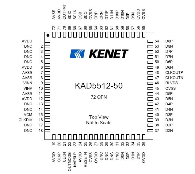
KAD5512P-50: Features: • Programmable gain, offset and skew control• 1.3 GHz analog input bandwidth• 52fs Clock Jitter• Over-range indicator• Selectable Clock Divider: ÷1 or ÷2̶...

floor Price/Ceiling Price

Part Number:
KAD5512P-50
Supply Ability:
5000

Price Break

  • Qty
  • 1~5000
  • Unit Price
  • Negotiable
  • Processing time
  • 15 Days
Total Cost: $ 0.00

SeekIC Buyer Protection PLUS - newly updated for 2013!

  • Escrow Protection.
  • Guaranteed refunds.
  • Secure payments.
  • Learn more >>

Month Sales

268 Transactions

Rating

evaluate  (4.8 stars)

Upload time: 2024/4/25

Payment Methods

All payment methods are secure and covered by SeekIC Buyer Protection PLUS.

Notice: When you place an order, your payment is made to SeekIC and not to your seller. SeekIC only pays the seller after confirming you have received your order. We will also never share your payment details with your seller.
Product Details

Description


Features:

• Programmable gain, offset and skew control
• 1.3 GHz analog input bandwidth
• 52fs Clock Jitter
• Over-range indicator
• Selectable Clock Divider: ÷1 or ÷2
• Clock Phase Selection
• Nap and Sleep modes
• Two's complement, Gray code or Binary data format
• DDR LVDS-compatible or LVCMOS outputs
• Programmable Built-in Test Patterns
• 1.8V Analog and Digital Supplies


Application

• Radar and Satellite Antenna Array Processing
• Broadband Communications
• High-Performance Data Acquisition


Pinout

  Connection Diagram


Specifications

Parameter Min Max Unit
AVDD to AVSS -0.4 2.1 V
OVDD to OVSS -0.4 2.1 V
AVSS to OVSS -0.4 0.3 V
Analog Inputs to AVSS -0.4 AVDD + 0.3 V
Clock Inputs to AVSS -0.4 AVDD + 0.3 V
Logic Input to AVSS -0.4 OVDD + 0.3 V
Logic Inputs to OVSS -0.4 OVDD + 0.3 V
Operating Temperature -0.4 85 °C
Storage Temperature -40 150 °C
Junction Temperature -65 150 °C
1. Exposing the device to levels in excess of the maximum ratings may cause permanent damage. Exposure to maximum conditions for extended periods may affect device reliability.


Description

The KAD5512P-50 is a low-power, high-performance, 12-bit, 500MSPS analog-to-digital converter designed with Intersils proprietary FemtoCharge™ technology on a standard CMOS process. The KAD5512P-50 is part of a pin-compatible portfolio of 10, 12 and 14-bit A/Ds with sample rates ranging from 125MSPS to 500MSPS. The device utilizes two time-interleaved 12-bit, 250MSPS A/D cores to achieve the ultimate sample rate of 500MSPS. A single 500MHz conversion clock is presented to the converter, and all interleave clocking is managed internally. A serial peripheral interface (SPI) port allows for extensive configurability, as well as fine control of matching characteristics (gain, offset, skew) between the two converter cores. These adjustments allow the user to minimize spurs associated with the interleaving process. Digital output data is presented in selectable LVDS or CMOS formats. The KAD5512P-50 is available in a 72-contact QFN package with an exposed paddle. Performance is specified over the full industrial temperature range (-40C to +85C).


Customers Who Bought This Item Also Bought

Margin,quality,low-cost products with low minimum orders. Secure your online payments with SeekIC Buyer Protection.
Circuit Protection
Motors, Solenoids, Driver Boards/Modules
Audio Products
Industrial Controls, Meters
Static Control, ESD, Clean Room Products
Line Protection, Backups
View more