KHC21025

Features: ·High-speed switching·No secondary breakdown·Very low on-resistance.PinoutSpecifications Parameter Symbol N-Channel P-Channel Unit Drain to Source Voltage VDSS 30 -30 V Gate to Source Voltage VGS ±20 ±20 V Drain Current Ts 80 ID 3...

product image

KHC21025 Picture
SeekIC No. : 004385362 Detail

KHC21025: Features: ·High-speed switching·No secondary breakdown·Very low on-resistance.PinoutSpecifications Parameter Symbol N-Channel P-Channel Unit Drain to Source Voltage VDSS ...

floor Price/Ceiling Price

Part Number:
KHC21025
Supply Ability:
5000

Price Break

  • Qty
  • 1~5000
  • Unit Price
  • Negotiable
  • Processing time
  • 15 Days
Total Cost: $ 0.00

SeekIC Buyer Protection PLUS - newly updated for 2013!

  • Escrow Protection.
  • Guaranteed refunds.
  • Secure payments.
  • Learn more >>

Month Sales

268 Transactions

Rating

evaluate  (4.8 stars)

Upload time: 2024/4/25

Payment Methods

All payment methods are secure and covered by SeekIC Buyer Protection PLUS.

Notice: When you place an order, your payment is made to SeekIC and not to your seller. SeekIC only pays the seller after confirming you have received your order. We will also never share your payment details with your seller.
Product Details

Description


Features:

·High-speed switching
·No secondary breakdown
·Very low on-resistance.


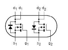
Pinout

  Connection Diagram


Specifications

Parameter
Symbol
N-Channel
P-Channel
Unit
Drain to Source Voltage
VDSS
30
-30
V
Gate to Source Voltage
VGS
±20
±20
V
Drain Current Ts 80
ID
3.5
-2.3
A
peak drain current *1
total power dissipation Ts = 80 ; *2
Tamb= 25 ; * 3
Tamb = 25 ; * 4
Tamb = 25 ; * 5
Ptot
2
W
2
1
1.3
storage temperature
Tstg
-65 to 150
operating junction temperature
Tj
150
source current (DC) Ts 80
IS
1.5
1.25
A
peak pulsed source current *1
ISM
6
-5
A
thermal resistance from junction to soldering point
Rth j-s
35
K/W
*1 Pulse width and duty cycle limited by maximum junction temperature.
*2 Maximum permissible dissipation per MOS transistor. Both devices may be loaded up to 2 W at the same time.
*3 Maximum permissible dissipation per MOS transistor. Device mounted on printed-circuit board with an Rth a-
t (ambient to tie-point) of 27.5 K/W.
*4 Maximum permissible dissipation per MOS transistor. Device mounted on printed-circuit board with an Rth a-
tp (ambient to tie-point) of 90 K/W.
*5 Maximum permissible dissipation if only one MOS transistor dissipates. Device mounted on printed-circuit
board with an Rth a-tp (ambient to tie-point) of 90 K/W.


Customers Who Bought This Item Also Bought

Margin,quality,low-cost products with low minimum orders. Secure your online payments with SeekIC Buyer Protection.
Motors, Solenoids, Driver Boards/Modules
Tapes, Adhesives
803
Resistors
Cable Assemblies
Power Supplies - External/Internal (Off-Board)
View more