L29C525

Features: ·Dual 8-Deep Pipeline Register ·Configurable to Single 16-Deep ·Low Power CMOS Technology ·Replaces AMD Am29525 ·Load, Shift, and Hold Instructions·Separate Data In and Data Out Pins ·Three-State Outputs ·Package Styles Available:·28-pin Plastic DIP·28-pin Plastic LCC, J-LeadPinoutDescri...

product image

L29C525 Picture
SeekIC No. : 004389031 Detail

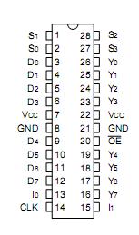
L29C525: Features: ·Dual 8-Deep Pipeline Register ·Configurable to Single 16-Deep ·Low Power CMOS Technology ·Replaces AMD Am29525 ·Load, Shift, and Hold Instructions·Separate Data In and Data Out Pins ·Thre...

floor Price/Ceiling Price

Part Number:
L29C525
Supply Ability:
5000

Price Break

  • Qty
  • 1~5000
  • Unit Price
  • Negotiable
  • Processing time
  • 15 Days
Total Cost: $ 0.00

SeekIC Buyer Protection PLUS - newly updated for 2013!

  • Escrow Protection.
  • Guaranteed refunds.
  • Secure payments.
  • Learn more >>

Month Sales

268 Transactions

Rating

evaluate  (4.8 stars)

Upload time: 2024/4/18

Payment Methods

All payment methods are secure and covered by SeekIC Buyer Protection PLUS.

Notice: When you place an order, your payment is made to SeekIC and not to your seller. SeekIC only pays the seller after confirming you have received your order. We will also never share your payment details with your seller.
Product Details

Description


Features:

·Dual 8-Deep Pipeline Register
·Configurable to Single 16-Deep
·Low Power CMOS Technology
·Replaces AMD Am29525
·Load, Shift, and Hold Instructions
·Separate Data In and Data Out Pins
·Three-State Outputs
·Package Styles Available:
·28-pin Plastic DIP
·28-pin Plastic LCC, J-Lead


Pinout

  Connection Diagram


Description

The L29C525 is a high-speed, low power CMOS pipeline register.  L29C525 is pin-for-pin compatible with the AMD Am29525.  The L29C525  can be configured as two independent 8-level pipelines or as a single 16-level pipeline.  The configuration imple- men ted is determined by the instruc- tion code (I1-0) as shown in Table 2. 

The I internal routing of data and l oading of each register.  For instruction I 1-0 = 00 (Push A and B), data  applied at the D7-0 inputs is latched into register A0 on the rising edge of CLK.  The contents of A0 simultaneously move to register A1, A1 moves to A2, and so on.  The contents of register A7 are wrapped back to register B0.  The registers on the B side are similarly shifted, with the contents of register B7 lost.

Instruction I1-0 = 01 (Push B) acts similarly to the Push A and B instruction, except that only the B side registers are shifted.  The input data is applied to register B0, and the contents of register B7 are lost.  The contents of the A side registers are unaffected.  Instruction I1-0 = 10 (Push A) is identical to the Push B  instruction, except that the A side  registers are shifted and the B side registers are unaffected.


Instruction I1-0 = 11 (Hold) causes no internal data movement.  It is equiva- lent to preventing the application of a clock edge to any internal register.

The contents of any of the registers is selectable at the output through the use of the S3-0 control inputs.  The in dependence of the I and S control lines allows simultaneous reading and writing.  Encoding for the S3-0 controls is given in Table 3.


Customers Who Bought This Item Also Bought

Margin,quality,low-cost products with low minimum orders. Secure your online payments with SeekIC Buyer Protection.
Motors, Solenoids, Driver Boards/Modules
Industrial Controls, Meters
Audio Products
Transformers
Isolators
View more