LC866436B

Features: (1) Read-Only Memory (ROM) : LC866448B 49152 × 8 bits : LC866444B 45056 × 8 bits : LC866440B 40960 × 8 bits : LC866436B 36864 × 8 bits : LC866432B 32768 × 8 bits : LC866428B 28672 × 8 bits : LC866424B 24576 × 8 bits: LC866420B 20480 × 8 bits : LC866416B 16384 × 8 bits : LC866412B ...

product image

LC866436B Picture
SeekIC No. : 004392395 Detail

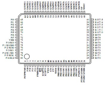
LC866436B: Features: (1) Read-Only Memory (ROM) : LC866448B 49152 × 8 bits : LC866444B 45056 × 8 bits : LC866440B 40960 × 8 bits : LC866436B 36864 × 8 bits : LC866432B 32768 × 8 bits : LC866428B 28672 × 8 ...

floor Price/Ceiling Price

Part Number:
LC866436B
Supply Ability:
5000

Price Break

  • Qty
  • 1~5000
  • Unit Price
  • Negotiable
  • Processing time
  • 15 Days
Total Cost: $ 0.00

SeekIC Buyer Protection PLUS - newly updated for 2013!

  • Escrow Protection.
  • Guaranteed refunds.
  • Secure payments.
  • Learn more >>

Month Sales

268 Transactions

Rating

evaluate  (4.8 stars)

Upload time: 2024/4/27

Payment Methods

All payment methods are secure and covered by SeekIC Buyer Protection PLUS.

Notice: When you place an order, your payment is made to SeekIC and not to your seller. SeekIC only pays the seller after confirming you have received your order. We will also never share your payment details with your seller.
Product Details

Description


Features:

(1) Read-Only Memory (ROM)                                          : LC866448B 49152 × 8 bits
                                                                                        : LC866444B 45056 × 8 bits
                                                                                        : LC866440B 40960 × 8 bits
                                                                                        : LC866436B 36864 × 8 bits
                                                                                        : LC866432B 32768 × 8 bits 
                                                                                        : LC866428B 28672 × 8 bits
                                                                                        : LC866424B 24576 × 8 bits 
                                                                                        : LC866420B 20480 × 8 bits
                                                                                        : LC866416B 16384 × 8 bits
                                                                                        : LC866412B 12288 × 8 bits
                                                                                        : LC866408B 8192 × 8 bits
(2) Random Access Memory (RAM)                                   : LC866448B/44B/40B/36B 1152 × 8 bits
                                                                                        : LC866432B/28B/24B 768 × 8 bits
                                                                                        : LC866420B/16B 640 × 8 bits
                                                                                        : LC866412B/08B 512 × 8 bits
(3) Bus Cycle Time/Instruction Cycle Time
The LC866448B/44B/40B/36B/32B/28B/24B/20B/16B/12B/08B are constructed to read ROM twice within one instruction cycle. It has 1.7 times more performance capability within the same instruction cycle compared to our 4-bit microcomputers (LC66000 series). Bus cycle time indicates the speed to read ROM.

Bus cycle time
Cycle time
Clock divider
System clock oscillation
Oscillation Frequency
Voltage
0.5µs
1µs
1/1
Ceramic resonator oscillation
6MHz
4.5V to 6.0V
2µs
4µs
1/1
Ceramic resonator oscillation
3MHz
2.5V to 6.0V
7.5µs
15µs
1/1
RC resonator oscillation
800kHz
2.5V to 6.0V
183µs
366µs
1/2
Crystal oscillation
32.768kHz
2.5V to 6.0V
(4) Ports
   - Input/output ports                                           :  1 port (8 terminals : port 1)
   Input/output programmable in a bit
   - 15V withstand Input/Output ports                   :  2 ports (12 terminals)
  Input/output port programmable in nibble unit   :  1 port (8 terminals : port 0)
  (When the N-channel open drain output is selected, the data in a bit can be inputted.)  
  Input/output port programmable in a bit             :  1 port (4 terminals : port 3)
  - Input port                                                          :  2 ports (14 terminals : port 7,8)  
  - VFD output port                                                 :  38 terminals
  Large current output for digit                               :  16 terminals
  Pull-down resistor option available
  - Other function
  Input/output port                                                 :  1 port (6 terminals : port E)
  Input port                                                             :  2 ports (16 terminals : port C,D)  
(5) VFD automatic dislay controller
  -Segment/digit output pattern programmable
  Any segment/digit combination available
  VFD parallel-drive available
  - 16-step dimmer function available

(6) AD converter 
  - 8-channel × 8-bit AD converter
(7) Serial-interface
  - 1 channel × 16-bit serial-interface circuits
  - 1 channel × 8-bit serial-interface circuits
  - LSB first / MSB first function available
  - Internal 8-bit baud-rate generator in common with two serial-interface circuits
(8) Timer
  - Timer 0
    16-bit timer/counter
    2-bit prescaler + 8-bit programmable prescaler
      Mode 0 : Two 8-bit timers with programmable prescaler
      Mode 1 : 8-bit timer with programmable prescaler + 8-bit counter
      Mode 2 : 16-bit timer with programmable prescaler
      Mode 3 : 16-bit counter
         The resolution of Timer is tCYC. (tCYC: cycle time)  
  - Timer 1
   16-bit timer/PWM
      Mode 0 : Two 8-bit timers 
      Mode 1 : 8-bit timer + 8-bit PWM
      Mode 2 : 16-bit timer  
      Mode 3 : Variable-bit PWM (9-16 bits)
          In Mode 0 and Mode 1,the resolution of Timer and PWM is tCYC. 
          In Mode 2 and Mode 3,the resolution of Timer and PWM selectable: tCYC or 1/2 tCYC by program
  - Base timer
    Every 500ms overflow system for a clock application (using 32.768kHz crystal oscillation for Base timer clock)
    Every 976µs, 3.9ms, 15.6ms, 62.5ms overflow system (using 32.768kHz crystal oscillation for Base timer clock)
    The Base timer clock selectable; 32.768kHz crystal oscillation, System clock, and programmable prescaler output of Timer 0
(9) Buzzer output
   - The Buzzer sound frequency selectable; 4KHz, 2KHz (using 32.768kHz crystal oscillation for Base timer clock)  
(10) Remote-control receiver circuit (Shares with the P73/INT3/T0IN terminal)
    - Noise Rejection function (the time constant of noize rejection filter: 1tCYC/16tCYC/64tCYC)
                                           (tCYC: instruction cycle time)
    - Switch Polarity function  
(11) Watchdog timer
   - The watchdog timer is taken on RC outside
   - Watchdog timer operation selectable: interrupt system, system reset    
(12) Interrupt system
   - 14-source 10-vectored interrupts :
      1. External interrupt INT0 (include watchdog timer)
      2. External interrupt INT1
      3. External interrupt INT2, Timer/counter T0L (Lower 8-bit)
      4. External interrupt INT3, Base timer  
      5. Timer/counter T0H (Upper 8-bit)
      6. Timer T1L, Timer T1H
      7. Serial-interface SIO0
      8. Serial-interface SIO1
      9. AD converter
     10. VFD automatic display controller, Port 0
   - Built-in Interrupt Priority control register
      Microcontroller allows 3 levels of interrupt; low level, high level, and highest level of multiplex interrupt. It can
      specify a low level or a high level interrupt priority from INT2/T0L through port 0 
      (i.e. the above interrupt number from three through ten). It can also specify a low level or the highest level interrupt
      priority to INT0 and INT1.
(13) Real-time service operation
       The Real-Time Service (RTS) functions the 4-byte data-transfer between the Special Function Registers at
       acknowledging the interrupt request.
       The RTS starts within 1 instruction cycle-time and completes within 5 instructions cycle-time after occurring the
       interrupt request.
(14) Subroutine stack levels
      - 128 levels (Max.): Stack area included in RAM area
(15) Multiplication and division
      16-bit × 8-bit (7 instruction cycle times)
      16-bit / 8-bit (7 instruction cycle times)
(16) Three oscillation circuits
     - On-chip RC oscillation circuit using for the system clock.
     - On-chip CF oscillation circuit using for the system clock. 
     - On-chip crystal oscillation circuit using for the system clock and for time-base clock.
(17) Standby function
     - HALT mode function
     The HALT mode is used to reduce power dissipation. In this operation mode, program execution is stopped. This
     operation mode can be released by interrupt request signals or the initial system reset request signal.
     - HOLD mode function
     The HOLD mode is used to freeze all the oscillations;
     RC (internal), CF and Crystal oscillations. This mode can be released by the following operations.
      • Reset terminal ( RES ) set to Low level
      • P70/INT0/T0IN, P71/INT1/T0IN terminals set to assigned level (programmable)
      • Input a Port 0 interrupt condition
(18) Factory shipment
      • QFP80E delivery form
(19) Development support tools
         Evaluation (EVA) chip  :  LC866097
         EPROM version  :   LC86E6449
         One time version  :  LC86P6449
         Emulator  :  EVA-86000 + ECB866400 (Evaluation chip board) + POD866400 (POD)


Pinout

  Connection Diagram


Customers Who Bought This Item Also Bought

Margin,quality,low-cost products with low minimum orders. Secure your online payments with SeekIC Buyer Protection.
Potentiometers, Variable Resistors
LED Products
Tapes, Adhesives
803
Integrated Circuits (ICs)
View more