Features: · 50 MHz Maximum Operating Frequency· Programmable Buffer Length from 2 to 2049 Clock Cycles· 10-bit Data Inputs and Outputs· Data Delay and Data Recirculation Modes·Supports Positive or Negative Edge System Clocks· Expandable Data Word Width or Buffer Length· 44-pin PLCC, J-LeadPinoutSp...
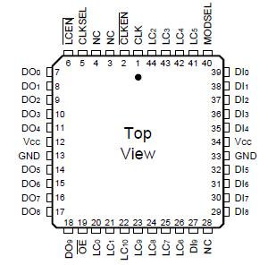
LF9502: Features: · 50 MHz Maximum Operating Frequency· Programmable Buffer Length from 2 to 2049 Clock Cycles· 10-bit Data Inputs and Outputs· Data Delay and Data Recirculation Modes·Supports Positive or N...
SeekIC Buyer Protection PLUS - newly updated for 2013!
268 Transactions
All payment methods are secure and covered by SeekIC Buyer Protection PLUS.
Storage temperature .......................................................65 to +150
Operating ambient temperature .......................................55to +125
VCC supply voltage with respect to ground ........................... 0.5 V to +7.0 V
Input signal with respect to ground ................................0.5 V to VCC + 0.5 V
Signal applied to high impedance output ........................ 0.5 V to VCC + 0.5 V
Output current into low outputs .................................................................25 mA
Latchup current .................................................................................... > 400 mA
The LF9502 is a high-speed, 10-bit programmable line buffer. Some applications the LF9502 is useful for include sample rate conversion, data time compression/expansion, software controlled data alignment, and programmable serial data shifting. By using the MODSEL pin, two different modes of operation can be selected: delay mode and data recirculation mode. The delay mode provides a minimum of 2 to a maximum of 2049 clock cycles of delay between the input and output of the device. The data recirculation mode provides a feedback path from the data output to the data input for use as a programmable circular buffer.
By using the length control input (LC10-0) and the length control enable (LCEN ) the length of the delay buffer or amount of recirculation delay canbe programmed. Providing a delay value on the LC10-0 inputs and driving LCEN LOW will load the delay value into the length control register on the next selected clock edge. Two registers, one preceeding the programmable delay RAM and one following, are included in the delay path. Therefore, the programmed delay value should equal the desired delay minus 2. This consequently means that the value loaded into the length control register must range from 0 to 2047 (to provide an overall range of 2 to 2049).
The active edge of the clock input, either positive or negative edge, can be selected with the clock select (CLKSEL) input. All timing is based on the active clock edge selected by CLKSEL. Data can be held temporarily by using the clock enable (CLKEN ) input.