Features: • Very High-Performance Read
85 ns Maximum Access Time
• High-Density Symmetrically Blocked Architecture
Sixteen 64K Blocks
• Extended Cycling Capability
100,000 Block Erase Cycles
1.6 Million Block Erase Cycles per Chip
• Automated Byte Write and Block Erase
Command User Interface
Status Register
• System Performance Enhancements
Ry/By Status Output
Erase Suspend Capability
• Deep-Powerdown Mode
0.20 A ICC Typical
• SRAM-Compatible Write Interface
• Hardware Data Protection Feature
Erase/Write Lockout during Power Transitions
• Independent Software Vendor Support
Microsoft Flash File System™ (FFS)
• ETOX™ Nonvolatile Flash Technology
12 V Byte Write/Block Erase
• Industry Standard Packaging
40-Pin 1.2 mm * 10 mm * 20 mm TSOP (Type I) Package
44-Pin 600-mil SOP Package
Pinout Specifications
Operating Temperature
During Read ....................................... 0 to +70 1
During Block Erase/Byte Write ............... 0 to +70
Temperature Under Bias ..................... 10 to +80
Storage Temperature ........................-65 to +125
Voltage on Any Pin (except VCC and VPP)
with Respect to GND .................... -2.0 V to +7.0 V2
VPP Program Voltage with Respect to GND during
Block Erase/Byte Write ............-2.0 V to +14.0 V2, 3
VCC Supply Voltage with Respect
to GND.......................................... -2.0 V to +7.0 V2
Output Short Circuit Current ......................... 100 mA4
DescriptionThe LH28F008SA is a high-performance 8M (8,388,608 bit) memory organized at 1M (1,048,576 bytes) of 8 bits each. Sixteen 64K (65,536 Byte) blocks are included on the LH28F008SA. A memory map is shown in Figure 4 of this specification. A block erase operation erases one of the sixteen blocks of memory in typically 1.6 seconds, independent of the remaining blocks. Each block can be independently erased and written 100,000 cyles. Erase Suspend mode allows system software to suspend block erase to read data or execute code from any other block of the LH28F008SA.
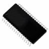
The LH28F008SA is available in the 40-pin TSOP (Thin Small Outline Package, 1.2 mm thick) package. Pinouts are shown in Figure 1 of this specification.
The Command User Interface serves as the interface between the microprocessor or microcontroller and the internal operation of the LH28F008SA. Byte Write and Block Erase Automation allow byte write and block erase operations to be executed using a two-write command sequence to the Command User Interface. The internal Write State Machine (WSM) automatically executes the algorithms and timings necessary for byte write and block erase operations, including verifications, thereby unburdening the microprocessor or microcontroller. Writing of memory data is performed in byte increments typically within 9 s, an 80% improvement over current flash memory products. IPP byte write and block erase currents are 10 mA typical, 30 mA maximum. VPP byte write and block erase
voltage is 11.4 V to 12.5 V.
The Status Register indicates the status of the WSM and when the WSM successfully completes the desired byte write or block erase operation.

 LH28F008SA Data Sheet