Series: -
Operating Temperature: -40°C ~ 85°C
Format - Memory: FLASH
Voltage - Supply: 2.7 V ~ 3.6 V
Interface: Parallel
Packaging: Tray
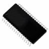
Supplier Device Package: 48-TSOP
Speed: 90ns
Memory Size: 16M (2M x 8, 1M x 16)
Manufacturer: Sharp Microelectronics
Memory Type: Boot Block FLASH
Package / Case: 48-TSOP
Features: Key enhancements of LH28F800BVHE-BTL90 Smart3 Flash memory are:
·Smart3 Technology
·Enhanced Suspend Capabilities
·Boot Block Architecture
Please note following important differences:
*VPPLK has been lowered to 1.5V to support 2.7V-3.6V block erase and word/byte write operations. The Vpp voltage transitions to GND is recommended for designs that switch VFF off during read operation.
*To take advantage of Smart3 technology, allow Vcc and Vpp connection to 2.7V-3.6V.
SpecificationsOperating Temperature
During Read, Block Erase
Full Chip Erase, Word/Byte Write
and Lock-Bit Configuration. . -40 to +85(1)
Storage Temperature
During under Bias . . . .. . . . . . . -40 to +85
During non Bias . . . . . . . . .. . . -65 to +125
Voltage On Any Pin
(except Vcc and Vccw) . . - 0.5v to Vcc +0.5V(2)
Vcc Supply Voltage . . . . . . . .. . . -0.2V to +4.6V(2)
Vcc Supply Voltage . . . . . . . .. -0.2V to +13.0V(2,3)
Output Short Circuit Current . . . . . .. . . . .l00mA(4)
NOTES:
1. Operating temperature is for commercial temperature product defined by this specification.
2. All specified voltages are with respect to GND. Minimum DC voltage is -0.5V on input/output pins and -0.2V on Vcc and Vccw pins. During transitions, this level may undershooto -2.0V for periods <20ns. Maximum DC voltage on input/output pins are Vcc+0.5V which, during transitions. may overshoot to Vcc+2.0V for periods <20ns.
3. Maximum DC voltage on Vcc may overshoot to+13.0V for periods <20ns. Applying 12V±0.3V to
Vccw during erase/write can only be done for a maximum of 1000 cycles on each block. Vccw may be connected to 12V±0.3V for a total of 80 hours maximum.
4. Output shorted for no more than one second. No more than one output shorted at a time.

 LH28F160BJHE-TTL90 Data Sheet