Features: −3 dB BW 150 MHz
Gain control BW 100 MHz
Adjustment range (<10 MHz) 80 dB
Gain matching (limit) ±0.50 dB
Supply voltage range 7V to 12V
Slew rate (inverting) 1500 V/s
Supply current (no load) 11 mA
Linear output current ±60 mA
Output voltage swing ±2.4V
Input noise voltage 4.4 nV/
Input noise current 2.6 pA/
THD (20 MHz, RL = 100, VO = 2 VPP) −45 dBcApplication Variable attenuator
AGC
Voltage controlled filter
Video imaging processingSpecifications
| Gain Adjust Range |
80 dB |
| Analog Control BW |
150 MHz |
| Signal Channel BW |
150 MHz |
| Supply Min |
7 Volt |
| Supply Max |
12 Volt |
| Gain Control Interface |
Voltage |
| Slew Rate |
1500 Volts/usec |
| Supply Current |
11 mA |
| PowerWise Rating 2 |
73 uA/MHz |
| Output Current |
80 mA |
| Offset Voltage max, 25C |
55 mV |
| Max Input Bias Current |
3700 nA |
| Voltage Noise |
4.4 nV/root(Hz) |
| HD 2nd |
-47 dB |
| HD 3rd |
-55 dB |
| Diff Gain |
0.45 dB |
| Diff Phase |
0.13 % |
| Special Features |
Undefined |
| Function |
VGA |
| Temperature Min |
-40 deg C |
| Temperature Max |
85 deg C |
| PowerWise |
Yes |
| View Using Catalog |
ESD Tolerance (Note 4)
Human Body Model ....................................2000V
Machine Model .............................................200V
Input Current .............................................±10 mA
Output Current .............................120 mA (Note 3)
Supply Voltages (V+ - V−) .............................12.6V
Voltage at Input/ Output pins .V+ +0.8V, V− −0.8V
Storage Temperature Range ........−65°C to 150°C
Junction Temperature ..................................150°C
Soldering Information:
Infrared or Convection (20 sec)................ 235°C
Wave Soldering (10 sec)........................... 260°CDescriptionThe LMH6505 is a wideband DC coupled voltage controlled gain stage followed by a high speed current feedback operational amplifier which can directly drive a low impedance load. The gain adjustment range is 80 dB for up to 10 MHz which is accomplished by varying the gain control input voltage, VG.
Maximum gain is set by external components, and the gain can be reduced all the way to cutoff. Power consumption is 110 mW with a speed of 150 MHz and a gain control bandwidth (BW) of 100 MHz. Output referred DC offset voltage is less than 55 mV over the entire gain control voltage range. Device-to-device gain matching is within ±0.5 dB at maximum gain. Furthermore, gain is tested and guaranteed over a wide range. The output current feedback op amp allows high frequency large signals (Slew Rate = 1500 V/s) and can also drive a heavy load current (60 mA) guaranteed. Near ideal input characteristics (i.e. low input bias current, low offset, low pin 3 resistance) enable the device to be easily configured as an inverting amplifier as well.
To provide ease of use when working with a single supply, the VG range is set to be from 0V to +2V relative to the ground pin potential (pin 4). VG input impedance is high in order to ease drive requirement. In single supply operation, the ground pin is tied to a "virtual" half supply.
The LMH6505's gain control is linear in dB for a large portion of the total gain control range from 0 dB down to −85 dB at 25°C, as shown below. This makes the device suitable for AGC applications. For linear gain control applications, see the LMH6503 datasheet.
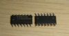
The LMH6505 is available in either the 8-Pin SOIC or the 8-Pin MSOP package. The combination of minimal external components and small outline packages allows the LMH6505 to be used in space-constrained applications.
Reliability Metrics
| Part Number |
Process |
EFR Reject |
EFR Sample Size |
PPM |
LTA Rejects |
LTA Device Hours |
FITS |
MTTF (Hours) |
| LMH6505MA |
VIP 10 |
0 |
11856 |
0 |
0 |
1065000 |
4 |
302196657 |
| LMH6505MAX |
VIP 10 |
0 |
11856 |
0 |
0 |
1065000 |
4 |
302196657 |
| LMH6505MM |
VIP 10 |
0 |
11856 |
0 |
0 |
1065000 |
4 |
302196657 |
| LMH6505MMX |
VIP 10 |
0 |
11856 |
0 |
0 |
1065000 |
4 |
302196657 |
Note: The Early Failure Rates (EFR) were calculated as point estimate PPM based on rejects and sample size for EFR. The Long Term Failure Rates were calculated at 60% confidence using the Arrhenius equation at 0.7eV activation energy and derating the assumed stress temperature of 150°C to an application temperature of 55°C.For more information on Reliability Metrics, please click here.
Reference Designs
| • |
RD-162 - Precision Amplitude Control for Analog Video |

 LMH6505 Data Sheet