LSI53C895

Features: · SCSI Performance· PCI Performance· Integration· Ease of Use· Flexibility· Reliability· TestabilityPinoutDescriptionThis chapter presents the LSI53C895 pin configurations and signal definitions by using tables and illustrations. Figure 4.1 is the functional signal grouping for the LSI53...

product image

LSI53C895 Picture
SeekIC No. : 004400070 Detail

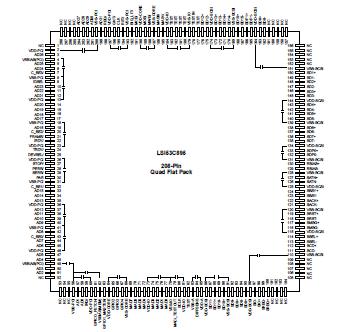
LSI53C895: Features: · SCSI Performance· PCI Performance· Integration· Ease of Use· Flexibility· Reliability· TestabilityPinoutDescriptionThis chapter presents the LSI53C895 pin configurations and signal defin...

floor Price/Ceiling Price

Part Number:
LSI53C895
Supply Ability:
5000

Price Break

  • Qty
  • 1~5000
  • Unit Price
  • Negotiable
  • Processing time
  • 15 Days
Total Cost: $ 0.00

SeekIC Buyer Protection PLUS - newly updated for 2013!

  • Escrow Protection.
  • Guaranteed refunds.
  • Secure payments.
  • Learn more >>

Month Sales

268 Transactions

Rating

evaluate  (4.8 stars)

Upload time: 2024/3/27

Payment Methods

All payment methods are secure and covered by SeekIC Buyer Protection PLUS.

Notice: When you place an order, your payment is made to SeekIC and not to your seller. SeekIC only pays the seller after confirming you have received your order. We will also never share your payment details with your seller.
Product Details

Description


Features:

· SCSI Performance
· PCI Performance
· Integration
· Ease of Use
· Flexibility
· Reliability
· Testability


Pinout

  Connection Diagram


Description

This chapter presents the LSI53C895 pin configurations and signal definitions by using tables and illustrations. Figure 4.1 is the functional signal grouping for the LSI53C895. The pin definitions are in Table 4.1 through Table 4.12. These definitions are organized into the following functional groups: System, Address/Data, Interface Control, Arbitration,  Error Reporting, SCSI, and Optional Interface.

This chapter includes these main topics:
` Section 4.1, "Voltage Capabilities and Limitations," page 4-3
` Section 4.2, "Internal Pull-ups on LSI53C895 Pins," page 4-4
` Section 4.3, "Pin Descriptions," page 4-5

A slash (/) at the end of the signal name indicates that the active state occurs when the signal is at a LOW voltage. When the slash is absent, the signal is active at a HIGH voltage.


Customers Who Bought This Item Also Bought

Margin,quality,low-cost products with low minimum orders. Secure your online payments with SeekIC Buyer Protection.
Circuit Protection
Cables, Wires
Prototyping Products
DE1
Computers, Office - Components, Accessories
View more