Series: -
Number of Converters: 1
Operating Temperature: -40°C ~ 85°C
Sampling Rate (Per Second): 200k
Packaging: Tube
Mounting Type: Through Hole
Number of Bits: 14
Data Interface: Serial, Parallel
Number of Inputs and Type: 2 Single-Ended, Unipolar; 2 Single-Ended, Bipolar; 1 Differential, Unipolar; 1 Differential, Bipolar
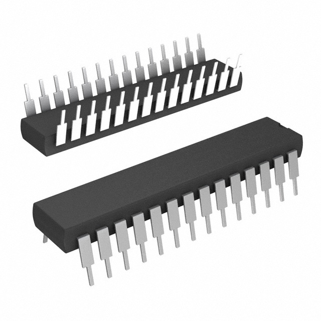
Package / Case: 28-DIP (0.300", 7.62mm)
Supplier Device Package: 28-PDIP
Voltage Supply Source: Dual ±
Manufacturer: Linear Technology
Power Dissipation (Max): 21.5mW Unipolar; 31.5mW Bipolar
Features: Single Supply 5V or ±5V Operation
Sample Rate: 200ksps
±1.25LSB INL and ±1LSB DNL Max
Power Dissipation: 15mW (Typ)
Parallel or Serial Data Output
No Missing Codes Over Temperature
Power Shutdown: Nap and Sleep
External or Internal Reference
Differential High Impedance Analog Input
Input Range: 0V to 4.096V or ±2.048V
81.5dB S/(N + D) and 94dB THD at Nyquist
28-Pin Narrow PDIP and SSOP Packages
ApplicationThe LTC1418 uses a successive approximation algorithm and an internal sample-and-hold circuit to convert an analog signal to a 14-bit parallel or serial output. The ADC is complete with a precision reference and an internal clock. The control logic provides easy interface to microprocessors and DSPs (please refer to Digital Interface section for the data format).
Conversion start is controlled by the CS and CONVST inputs. At the start of the conversion the successive approximation register (SAR) is reset. Once a conversion cycle has begun it cannot be restarted.
During the conversion, the internal differential 14-bit capacitive DAC output is sequenced by the SAR from the most significant bit (MSB) to the least significant bit (LSB).
Referring to Figure 1, the AIN+ and AIN inputs are connected to the sample-and-hold capacitors (CSAMPLE) during the acquire phase and the comparator offset is nulled by the zeroing switches. In this acquire phase, a minimum delay of 1ms will provide enough time for the sample-andhold capacitors to acquire the analog signal. During the convert phase the comparator zeroing switches open, putting the comparator into compare mode. The input switches the CSAMPLE capacitors to ground, transferring the differential analog input charge onto the summing junction. This input charge is successively compared with the binary weighted charges supplied by the differential capacitive DAC. Bit decisions are made by the high speed comparator. At the end of a conversion, the differential DAC output balances the AIN + and AIN input charges.
The SAR contents (a 14-bit data word) which represent the difference of AIN + and AIN are loaded into the 14-bit output latches. Pinout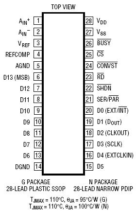 Specifications
Supply Voltage (VDD) ................................................. 6V
Negative Supply Voltage (VSS)
Bipolar Operation Only ........................... 6V to GND
Total Supply Voltage (VDD to VSS)
Bipolar Operation Only ....................................... ..12V
Analog Input Voltage (Note 3)
Unipolar Operation .................. 0.3V to (VDD + 0.3V)
Bipolar Operation........... (VSS 0.3V) to (VDD + 0.3V)
Digital Input Voltage (Note 4)
Unipolar Operation ................................0.3V to 10V
Bipolar Operation.........................(VSS 0.3V) to 10V
Digital Output Voltage
Unipolar Operation .................. ....0.3V to (VDD + 0.3V)
Bipolar Operation........... ....(VSS 0.3V) to (VDD + 0.3V)
Power Dissipation................................................ 500mW
Operation Temperature Range
LTC1418C................................................ 0°C to 70°C
LTC1418I............................................ 40°C to 85°C
Storage Temperature Range ................65°C to 150°C
Lead Temperature (Soldering, 10 sec)................... 300°C
DescriptionThe LTC
®1418 is a low power, 200ksps, 14-bit A/D converter. Data output is selectable for 14-bit parallel or serial format. This versatile device can operate from a single 5V or ±5V supply. An onboard high performance sample-and-hold, a precision reference and internal timing minimize external circuitry requirements. The low 15mW power dissipation is made even more attractive with two user selectable power shutdown modes.
The LTC1418 converts 0V to 4.096V unipolar inputs from a single 5V supply and ±2.048V bipolar inputs from ±5V supplies. DC specs include ±1.25LSB INL, ±1LSB DNL and no missing codes over temperature. Outstanding AC performance includes 82dB S/(N + D) and 94dB THD at the Nyquist input frequency of 100kHz.
The flexible output format of LTC1418 allows either parallel or serial I/O. The SPI/MICROWIRETM compatible serial I/O port can operate as either master or slave and can support clock frequencies from DC to 10MHz. A separate convert start input and a data ready signal (BUSY ) allow easy control of conversion start and data transfer.
Parameters: | Technical/Catalog Information | LTC1418AIN |
| Vendor | Linear Technology |
| Category | Integrated Circuits (ICs) |
| Number of Bits | 14 |
| Package / Case | 28-DIP (300 mil) |
| Data Interface | Serial/Parallel |
| Packaging | Tube |
| Sampling Rate (Per Second) | 200k |
| Operating Temperature | -40°C ~ 85°C |
| Voltage Supply Source | Dual ± |
| Number of Inputs and Type | 2 Single-Ended, Unipolar; 2 Single-Ended, Bipolar; 1 Differential, Unipolar; 1 Differential, Bipolar |
| Number of Converters | 1 |
| Power Dissipation (Max) | 21.5mW Unipolar; 31.5mW Bipolar |
| Drawing Number | 161; 05-08-1510; N; 8 |
| Lead Free Status | Contains Lead |
| RoHS Status | RoHS Non-Compliant |
| Other Names | LTC1418AIN
LTC1418AIN
|
 LTC1418AIN Data Sheet