LTC1693

Features: Dual MOSFET Drivers in SO-8 Packageor Single MOSFET Driver in MSOP Package 1GΩ Electrical Isolation Between the Dual DriversPermits High/Low Side Gate Drive 1.5A Peak Output Current 16ns Rise/Fall Times at VCC = 12V, CL = 1nF Wide VCC Range: 4.5V to 13.2V CMOS Compatible Inputs wi...

product image

LTC1693 Picture
SeekIC No. : 004401801 Detail

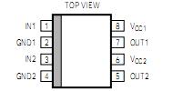
LTC1693: Features: Dual MOSFET Drivers in SO-8 Packageor Single MOSFET Driver in MSOP Package 1GΩ Electrical Isolation Between the Dual DriversPermits High/Low Side Gate Drive 1.5A Peak Output Current...

floor Price/Ceiling Price

Part Number:
LTC1693
Supply Ability:
5000

Price Break

  • Qty
  • 1~5000
  • Unit Price
  • Negotiable
  • Processing time
  • 15 Days
Total Cost: $ 0.00

SeekIC Buyer Protection PLUS - newly updated for 2013!

  • Escrow Protection.
  • Guaranteed refunds.
  • Secure payments.
  • Learn more >>

Month Sales

268 Transactions

Rating

evaluate  (4.8 stars)

Upload time: 2024/4/25

Payment Methods

All payment methods are secure and covered by SeekIC Buyer Protection PLUS.

Notice: When you place an order, your payment is made to SeekIC and not to your seller. SeekIC only pays the seller after confirming you have received your order. We will also never share your payment details with your seller.
Product Details

Description


Features:

Dual MOSFET Drivers in SO-8 Packageor Single MOSFET Driver in MSOP Package
1GΩ Electrical Isolation Between the Dual DriversPermits High/Low Side Gate Drive
1.5A Peak Output Current
16ns Rise/Fall Times at VCC = 12V, CL = 1nF
Wide VCC Range: 4.5V to 13.2V
CMOS Compatible Inputs with Hysteresis,Input Thresholds are Independent of VCC
Driver Input Can Be Driven Above VCC
Undervoltage Lockout
Thermal Shutdown


Application

Power Supplies
High/Low Side Drivers
Motor/Relay Control
Line Drivers
Charge Pumps


Pinout

  Connection Diagram


Specifications

Supply Voltage (VCC) ...............................................  14V
Inputs (IN, PHASE) ...................................  0.3V to 14V
Driver Output ................................  0.3V to VCC + 0.3V
GND1 to GND2 (Note 5) ......................................  ±100V
Junction Temperature..........................................  150°C
Operating Ambient Temperature Range .... 0°C to 70°C
Storage Temperature Range ...............65°C to 150°C
Lead Temperature (Soldering, 10 sec) ................. 300°C


Description

The LTC®1693 family drives power MOSFETs at highspeed. The 1.5A peak output current reduces switchinglosses in MOSFETs with high gate capacitance.

The LTC1693-1 contains two noninverting drivers. TheLTC1693-2 contains one noninverting and one invertingdriver. The LTC1693-1 and LTC1693-2 drivers are electri-cally isolated and independent. The LTC1693-3 is a singledriver with an output polarity select pin.

The LTC1693 has VCC independent CMOS input thresh-olds with 1.2V of typical hysteresis. The LTC1693 canlevel-shift the input logic signal up or down to the rail-to-rail VCC drive for the external MOSFET.

The LTC1693 contains an undervoltage lockout circuit anda thermal shutdown circuit. Both circuits disable theexternal N-channel MOSFET gate drive when activated.

The LTC1693-1 and LTC1693-2 come in an 8-lead SO pack-age. The LTC1693-3 comes in an 8-lead MSOP package.


Customers Who Bought This Item Also Bought

Margin,quality,low-cost products with low minimum orders. Secure your online payments with SeekIC Buyer Protection.
LED Products
Sensors, Transducers
Discrete Semiconductor Products
Hardware, Fasteners, Accessories
Power Supplies - Board Mount
Batteries, Chargers, Holders
View more