Features: ` Two-Wire I2C Serial Interface Supports 400 kHz Protocol
` Supply Voltage Ranges:
1.8V to 5.5V (M24512 − R)
2.5V to 5.5V (M24512 − W)
` Write Control Input
` BYTE and PAGE WRITE (up to 128 Bytes)
` RANDOM and SEQUENTIAL READ Modes
` Self-Timed Programming Cycle
` Automatic Address Incrementing
` Enhanced ESD/Latch-Up Protection
` More than 100,000 Erase/Write Cycles
` More than 40-Year Data RetentionPinout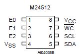 Specifications
|
Symbol |
Parameter |
Min. |
Max. |
Unit |
| TA |
Ambient Operating Temperature |
40 |
125 |
|
| TSTG |
Storage Temperature |
65 |
150 |
|
| TLEAD |
Lead Temperature during Soldering
|
See note 1 |
|
| VIO |
Input or Output range |
0.50 |
6.5 |
V |
| VCC |
Supply Voltage |
0.50 |
6.5 |
V |
| VESD |
Electrostatic Discharge Voltage (Human Body model) 2 |
-4000 |
4000 |
V |
Note: 1. Compliant with JEDEC Std J-STD-020C (for small body, Sn-Pb or Pb assembly), the ST ECOPACK® 7191395 specification, and the European directive on Restrictions on Hazardous Substances (RoHS) 2002/95/EU
2. AEC-Q100-002 (compliant with JEDEC Std JESD22-A114A, C1=100pF, R1=1500, R2=500)DescriptionThese I2C-compatible electrically erasable programmable memory (EEPROM) devices M24512 are organized as 64K x 8 bits.
I2C uses a two-wire serial interface M24512, comprising a bi-directional data line and a clock line. The devices carry a built-in 4-bit Device Type Identifier code (1010) in accordance with the I2C bus definition. The device behaves as a slave in the I2C protocol, with all memory operations synchronized by the serial clock. Read and Write operations are initiated by a Start condition, generated by the bus master master. The Start condition is followed by a Device Select Code and Read/Write bit (RW) (as described in Table 3.), terminated by an acknowledge bit.
When writing data to the memory, the M24512 inserts an acknowledge bit during the 9th bit time, following the bus master's 8-bit transmission. When data is read by the bus master, the bus master acknowledges the receipt of the data byte in the same way. Data transfers are terminated by a Stop condition after an Ack for Write, and after a NoAck for Read.
Power On Reset
In order to prevent data corruption and inadvertent Write operations during Power-up, a Power On Reset (POR) circuit is included. At Power-up, the device will not respond to any command until VCC has reached the Power On Reset threshold voltage (this threshold is lower than the VCC min operating voltage defined in Tables 8 and 9). In the same way, as soon as VCC drops from the normal operating voltage, below the Power On Reset threshold voltage, the device stops to respond to any command.
Prior to selecting and issuing commands to the memory M24512, a valid and stable VCC voltage must be applied. This voltage must remain stable and valid until the end of the transmission of the command and, for a Write instruction, until the completion of the internal write cycle (tW).

 M24512 Data Sheet