M2S56D30TP

Features: · Vdd=Vddq=2.5v±0.2V· Double data rate architecture; two data transfers per clock cycle· Bidirectional, data strobe (DQS) is transmitted/received with data· Differential clock inputs (CLK and /CLK)· DLL aligns DQ and DQS transitions with CLK transitions edges of DQS· Commands entered on ...

product image

M2S56D30TP Picture
SeekIC No. : 004404485 Detail

M2S56D30TP: Features: · Vdd=Vddq=2.5v±0.2V· Double data rate architecture; two data transfers per clock cycle· Bidirectional, data strobe (DQS) is transmitted/received with data· Differential clock inputs (CLK ...

floor Price/Ceiling Price

Part Number:
M2S56D30TP
Supply Ability:
5000

Price Break

  • Qty
  • 1~5000
  • Unit Price
  • Negotiable
  • Processing time
  • 15 Days
Total Cost: $ 0.00

SeekIC Buyer Protection PLUS - newly updated for 2013!

  • Escrow Protection.
  • Guaranteed refunds.
  • Secure payments.
  • Learn more >>

Month Sales

268 Transactions

Rating

evaluate  (4.8 stars)

Upload time: 2024/4/27

Payment Methods

All payment methods are secure and covered by SeekIC Buyer Protection PLUS.

Notice: When you place an order, your payment is made to SeekIC and not to your seller. SeekIC only pays the seller after confirming you have received your order. We will also never share your payment details with your seller.
Product Details

Description


Features:

· Vdd=Vddq=2.5v±0.2V
· Double data rate architecture; two data transfers per clock cycle
· Bidirectional, data strobe (DQS) is transmitted/received with data
· Differential clock inputs (CLK and /CLK)
· DLL aligns DQ and DQS transitions with CLK transitions edges of DQS
· Commands entered on each positive CLK edge;
· data and data mask referenced to both edges of DQS
· 4 bank operation controlled by BA0, BA1 (Bank Address)
· /CAS latency- 1.5/2.0/2.5 (programmable)
· Burst length- 2/4/8 (programmable)
· type- sequential / interleave (programmable)
· Auto precharge / All bank precharge controlled by A10
· 8192 refresh cycles /64ms (4 banks concurrent refresh)
· Auto refresh and Self refresh
· Row address A0-12 / Column address A0-9,11(x4)/ A0-9(x8)
· SSTL_2 Interface
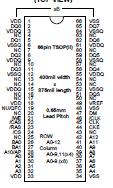
· 400-mil, 66-pin Thin Small Outline Package (TSOP II)
· FET switch control(/QFC)
· JEDEC standard


Pinout

  Connection Diagram


Specifications


Symbol
Parameter
Conditions
Ratings
Unit
Vdd Supply Voltage
with respect to Vss
-0.5 ~ 3.7
V
VddQ Supply Voltage for Output
with respect to VssQ
-0.5 ~ 3.7
V
VI Input Voltage
with respect to Vss
-0.5 ~ Vdd+0.5
V
VO Output Voltage
with respect to VssQ
-0.5~ VddQ+0.5
V
IO Output Current
50
mA
Pd Power Dissipation
Ta = 25
1000
mW
Topr Operating Temperature
0 ~ 70
Tstg Storage Temperature
-65 ~ 150


Description

M2S56D30TP is a 4-bank x 16777216-word x 4-bit, M2S56D30TP is a 4-bank x 8388608-word x 8-bit, double data rate synchronous DRAM, with SSTL_2 interface. All control and address signals are referenced to the rising edge of CLK. Input data is registered on both edges of data strobe, and output data and data strobe are referenced on both edges of CLK. The M2S56D30TP  achieves very high speed data rate up to 133MHz, and are suitable for main memory in computer systems.


Customers Who Bought This Item Also Bought

Margin,quality,low-cost products with low minimum orders. Secure your online payments with SeekIC Buyer Protection.
Audio Products
Transformers
Circuit Protection
Computers, Office - Components, Accessories
Power Supplies - Board Mount
View more