Features: ` Multi-Chip Package
1 die of 128 Mbit (8Mb x16, Mux I/O Multiple Bank, Multi-level, Burst) Flash Memory
1 die of 32 or 64Mbit Mux I/O, Burst Pseudo SRAM
` Supply voltage
VDDF = VDDP = VDDQF = 1.7 to 1.95V
VPPF = 9V for fast program
` Electronic signature
Manufacturer Code: 20h
Device Codes (Top Flash Configuration): M36L0R7060U1: 882Eh, M36L0R7050U1: 882Eh
Device Codes (Bottom Flash Configuration) M36L0R7060L1: 882Fh M36L0R7050L1: 882Fh
` ECOPACK® package
Flash memory
` Multiplexed address/data
` Synchronous / asynchronous read
Synchronous Burst Read mode: 66MHz
Random Access: 85ns
` Synchronous burst read suspend programming time
10s typical Word program time using Buffer Enhanced Factory Program command
` Memory organization
Multiple Bank Memory Array: 8 Mbit Banks
Parameter Blocks (Top or Bottom location)
` Security
64 bit unique device number
2112 bit user programmable OTP Cells
` 100,000 program/erase cycles per block
` Dual operations
program/erase in one Bank while read in others
No delay between Read and Write operations
` Block locking
All blocks locked at power-up
Any combination of blocks can be locked with zero latency
WPF for Block Lock-Down
Absolute Write Protection with VPPF = VSS
` Common Flash Interface (CFI)
PSRAM
` Access time: 70ns
` Synchronous modes:
Synchronous Write: continuous burst
Synchronous Read: continuous burst or fixed length: 4, 8 or 16 Words for 32 Mbit devices or 4, 8,16 or 32 Words for 64 Mbit devices
Maximum Clock Frequency: 83MHz
` Low power consumption
` Low power features
Partial Array Self-Refresh (PASR)
Deep Power-Down (DPD) Mode
Automatic Temperature-compensated Self- RefreshSpecificationsStressing the device above the rating listed in the Absolute Maximum Ratings table may cause permanent damage to the device. These are stress ratings only and operation of the device at these or any other conditions above those indicated in the Operating sections of this specification is not implied. Exposure to Absolute Maximum Rating conditions for extended periods may affect device reliability. Refer also to the STMicroelectronics SURE Program and other relevant quality documents.
| Symbol |
Parameter |
Value |
Unit |
|
Min |
Max |
| TA |
Ambient Operating Temperature |
-25 |
85 |
|
| TBIAS |
Temperature Under Bias |
-25 |
85 |
|
| TSTG |
Storage Temperature |
-55 |
125 |
|
| VIO |
Input or Output Voltage |
-0.2 |
2.45 |
V |
| VDDF,VDDQF,VCCP |
Core and Input/Output Supply Voltages |
-0.2 |
2.45 |
V |
| VPPF |
Flash Program Voltage |
-0.2 |
10 |
V |
| IO |
Output Short Circuit Current |
|
100 |
mA |
| tVPPFH |
Time for VPPF at VPPFH |
|
100 |
hours |
DescriptionThe M36L0R7060U1, M36L0R7060L1, M36L0R7050U1 and M36L0R7050L1 combine two memory devices in a Multi-Chip Package:
a 128-Mbit, Multiple Bank Flash memory, the M58LR128G(U/L)
a 32 or 64 Mbit PseudoSRAM, the M69KM048AA or M69KM096AA, respectively.
The purpose of this document M36L0R7060U1, M36L0R7060L1, M36L0R7050U1 and M36L0R7050L1 is to describe how the two memory components operate with respect to each other. M36L0R7060U1, M36L0R7060L1, M36L0R7050U1 and M36L0R7050L1 must be read in conjunction with the M58LRxxxGUL and M69KM048AA or M69KM096AA datasheets, where all specifications required to operate the Flash memory and PSRAM components are fully detailed. These datasheets are available from the STMicroelectronics website: www.st.com.
Recommended operating conditions of M36L0R7060U1, M36L0R7060L1, M36L0R7050U1 and M36L0R7050L1 do not allow more than one memory to be active at the same time.
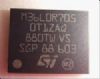
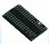
The memory M36L0R7060U1, M36L0R7060L1, M36L0R7050U1 and M36L0R7050L1 is offered in a Stacked TFBGA88 (8 *10mm, 8 * 10 ball array, 0.8mm pitch) package.
In order to meet environmental requirements, ST offers these devices in ECOPACK® packages. These packages of M36L0R7060U1, M36L0R7060L1, M36L0R7050U1 and M36L0R7050L1 have a Lead-free second-level interconnect. The category of Second-Level Interconnect is marked on the package and on the inner box label, in compliance with JEDEC Standard JESD97.
The maximum ratings of M36L0R7060U1, M36L0R7060L1, M36L0R7050U1 and M36L0R7050L1 related to soldering conditions are also marked on the inner box label. ECOPACK is an ST trademark. ECOPACK specifications are available at: www.st.com.

 M36L0R7050U1 Data Sheet