M67025

Features: • Fast Access Time: 30/45 ns• Wide Temperature Range: -55°C to +125°C• Separate Upper Byte and Lower Byte Control for Multiplexed Bus Compatibility• Expandable Data Bus to 32 bits or More Using Master/Slave Chip Select When Using More Than One Device• On-chi...

product image

M67025 Picture
SeekIC No. : 004406919 Detail

M67025: Features: • Fast Access Time: 30/45 ns• Wide Temperature Range: -55°C to +125°C• Separate Upper Byte and Lower Byte Control for Multiplexed Bus Compatibility• Expandable Data...

floor Price/Ceiling Price

Part Number:
M67025
Supply Ability:
5000

Price Break

  • Qty
  • 1~5000
  • Unit Price
  • Negotiable
  • Processing time
  • 15 Days
Total Cost: $ 0.00

SeekIC Buyer Protection PLUS - newly updated for 2013!

  • Escrow Protection.
  • Guaranteed refunds.
  • Secure payments.
  • Learn more >>

Month Sales

268 Transactions

Rating

evaluate  (4.8 stars)

Upload time: 2024/4/30

Payment Methods

All payment methods are secure and covered by SeekIC Buyer Protection PLUS.

Notice: When you place an order, your payment is made to SeekIC and not to your seller. SeekIC only pays the seller after confirming you have received your order. We will also never share your payment details with your seller.
Product Details

Description


Features:

• Fast Access Time: 30/45 ns
• Wide Temperature Range: -55°C to +125°C
• Separate Upper Byte and Lower Byte Control for Multiplexed Bus Compatibility
• Expandable Data Bus to 32 bits or More Using Master/Slave Chip Select When Using More Than One Device
• On-chip Arbitration Logic
• Versatile Pin Select for Master or Slave:
  M/S = H for Busy Output Flag On Master
  M/S = L for Busy Input Flag On Slave
• INT Flag for Port to Port Communication
• Full Hardware Support of Semaphore Signaling Between Ports
• Fully Asynchronous Operation From Either Port
• Battery Back-up Operation: 2V Data Retention
• TTL Compatible
• Single 5V + 10% Power Supply
• QML Q and V with SMD 5962-91617


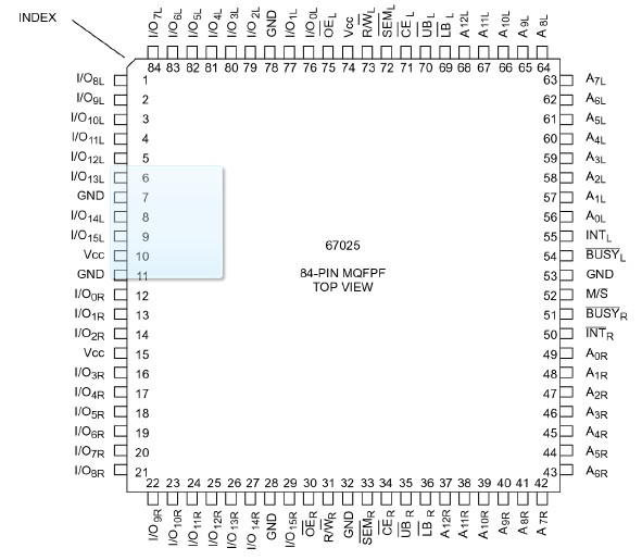
Pinout

  Connection Diagram


Description

The M67025E has two ports with separate control, address and I/O pins that permit independent read/write access to any memory location. M67025E has an automatic power-down feature controlled by CS. CS controls on-chip power-down circuitry which causes the port concerned to go into stand-by mode when not selected (CS high). When a port is selected access to the full memory array is permitted. Each port has its own Output Enable control (OE). In read mode, the port's OE turns the Output drivers on when set LOW. Non-conflicting READ/WRITE conditions are illustrated in Table 1.

The M67025E interrupt flag (INT) allows communication between ports or systems. If the user chooses to use the interrupt function, a memory location (mail box or message center) is assigned to each port. The left port interrupt flag (INTL) is set when the right port writes to memory location 1FFE (HEX). The left port clears the interrupt by reading address location 1FFE. Similarly, the right port interrupt flag (INTR) is set when the left port writes to memory location 1FFF (HEX), and the right port must read memory location 1FFF in order to clear the interrupt flag (INTR). The 16-bit message at 1FFE or 1FFF is userdefined. If the interrupt function is not used, address locations 1FFE and 1FFF are not reserved for mail boxes but become part of the RAM. See Table 3 for the interrupt function.


Customers Who Bought This Item Also Bought

Margin,quality,low-cost products with low minimum orders. Secure your online payments with SeekIC Buyer Protection.