Features: Industry Standard MICROWIRE Bus
Single Supply Voltage:
4.5 to 5.5V for M93Sx6
2.5 to 5.5V for M93Sx6-W
1.8 to 5.5V for M93Sx6-R
Single Organization: by Word (x16)
Programming Instructions that work on: Word or Entire Memory
Self-timed Programming Cycle with Auto-Erase
User Defined Write Protected Area
Page Write Mode (4 words)
Ready/Busy Signal During Programming
Speed:
1MHz Clock Rate, 10ms Write Time (Current product, identified by process identification letter F or M)
2MHz Clock Rate, 5ms Write Time (New Product, identified by process identification letter W or G)
Sequential Read Operation
Enhanced ESD/Latch-Up Behavior
More than 1 Million Erase/Write Cycles
More than 40 Year Data Retention
Pinout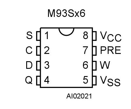 Specifications
|
Symbol |
Parameter |
Min. |
Max. |
Unit |
|
TSTG |
Storage Temperature |
65 |
150 |
|
|
TLEAD |
Lead Temperature during Soldering |
See note1 |
|
|
VOUT |
Output range (Q = VOH or Hi-Z) |
0.50 |
VCC+0.5 |
V |
|
VIN |
Input range |
0.50 |
VCC+1 |
V |
|
VCC |
Supply Voltage |
0.50 |
6.5 |
V |
|
VESD |
Electrostatic Discharge Voltage (Human Body model)2 |
4000 |
4000 |
V |
DescriptionThis specification covers a range of 4K, 2K, 1K bitserial Electrically Erasable Programmable Memo-ry (EEPROM)products (respectively for M93S66,M93S56, M93S46). In this text, these products arecollectively referred to as M93Sx6.
The M93Sx6 is accessed through a serial input (D)and output (Q) using the MICROWIRE bus proto-col. The memory is divided into 256, 128, 64 x16bit words (respectively for M93S66, M93S56,M93S46).
The M93Sx6 is accessed by a set of instructionswhich includes Read, Write, Page Write, Write Alland instructions used to set the memory protec-tion. These are summarized in Table 2. and Table3.).
A Read Data from Memory (READ) instructionloads the address of the first word to be read intoan internal address pointer. The data contained atthis address is then clocked out serially. The ad-dress pointer is automatically incremented afterthe data is output and, if the Chip Select Input (S)is held High, the M93Sx6 can output a sequentialstream of data words. In this way, the memory canbe read as a data stream from 16 to 4096 bits (forthe M93S66), or continuously as the addresscounter automatically rolls over to 00h when thehighest address is reached.
Within the time required by a programming cycle(tW), up to 4 words may be written with help of thePage Write instruction. the whole memory of M93S66, M93S56,M93S46 mayalso be erased, or set to a predetermined pattern,by using the Write Allinstruction. Within the memory, a user defined area may beprotected against further Write instructions. Thesize of this area is defined by the content of a Pro-tection Register, located outside of the memory ar-ray. As a final protection step, data may bepermanently protected by programming a OneTime Programming bit (OTP bit) which locks theProtection Register content.
Programming is internally self-timed (the externalclock signal on Serial Clock (C) may be stopped orleft running after the start of a Write cycle) anddoes not require an erase cycle prior to the Writeinstruction. The Write instruction writes 16 bits at atime into one of the word locations of the M93Sx6,the Page Write instruction writes up to 4 words of16 bits to sequential locations, assuming in bothcases that all addresses are outside the Write Pro-tected area. After the start of the programming cy-cle, a Busy/Ready signal is available on SerialData Output (Q) when Chip Select Input (S) is driv-en High.

 M93S46 Data Sheet


