Features:
♦ Excellent Dynamic Performance
69.9dB SNR at 5.3MHz
96dBc SFDR at 5.3MHz
95dB Channel Isolation
♦ Ultra-Low Power
96mW per Channel (Normal Operation)
♦ Serial LVDS Outputs
♦ Pin-Selectable LVDS/SLVS (Scalable Low-Voltage
Signal) Mode
♦ LVDS Outputs Support Up to 30 Inches FR-4
Backplane Connections
♦ Test Mode for Digital Signal Integrity
♦ Fully Differential Analog Inputs
♦ Wide Differential Input Voltage Range (1.4VP-P)
♦ On-Chip 1.24V Precision Bandgap Reference
♦ Clock Duty-Cycle Equalizer
♦ Compact, 100-Pin TQFP Package with Exposed
Paddle
♦ Evaluation Kit Available (Order MAX1437EVKIT)ApplicationUltrasound and Medical Imaging
Instrumentation
Multichannel CommunicationsPinout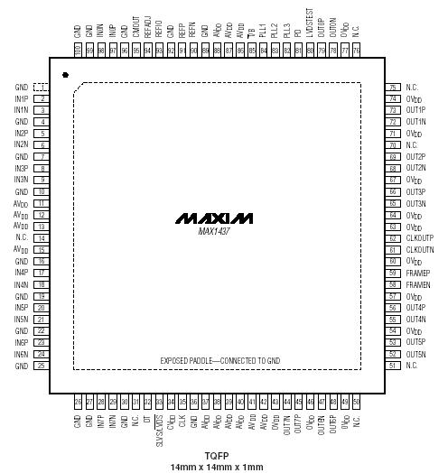 Specifications
AVDD to GND.........................................................-0.3V to +2.0V
CVDD to GND .......................................................-0.3V to +3.6V
OVDD to GND .......................................................-0.3V to +2.0V
IN_P, IN_N to GND...................................-0.3V to (AVDD + 0.3V)
CLK to GND..............................................-0.3V to (CVDD + 0.3V)
OUT_P, OUT_N, FRAME_,
CLKOUT_ to GND.....................................-0.3V to (OVDD + 0.3V)
DT, SLVS/LVDS, LVDSTEST, PLL_, T/B,
REFIO, REFADJ, CMOUT to GND ...............-0.3V to (AVDD + 0.3V)
Continuous Power Dissipation (TA = +70°C)
100-Pin TQFP 14mm x 14mm x 1mm
(derated 47.6mW/°C above +70°C)..........................3809.5mW
Operating Temperature Range ..........................-40°C to +85°C
Maximum Junction Temperature .....................................+150°C
Storage Temperature Range ............................65°C to +150°C
Lead Temperature (soldering, 10s) ...............................+300°C
DescriptionThe MAX1462 implements a revolutionary concept in signal conditioning, where the output of its 16-bit analog- to-digital converter (ADC) is digitally corrected over the specified temperature range. This feature can be readily exploited by automotive, industrial, and medical market segments, in applications such as sensors and smart batteries. Digital correction is provided by an internal digital signal processor (DSP) and on-chip 128- bit EEPROM containing user-programmed calibration coefficients. The conditioned output is available as a 12-bit digital word and as a ratiometric (proportional to the supply voltage) analog voltage using an on-board 12-bit digital-to-analog converter (DAC). The uncommitted op amp can be used to filter the analog output.
The analog front end of MAX1462 includes a 2-bit programmablegain amplifier (PGA) and a 3-bit coarse-offset (CO) DAC, which condition the sensor's output. This coarsely corrected signal is digitized by a 16-bit ADC. The DSP uses the digitized sensor signal, the temperature sensor, and correction coefficients stored in the internal EEPROM to produce the conditioned output.
Multiple or batch manufacturing of sensors is supported with a completely digital test interface. Built-in testability features on the MAX1462 result in the integration of three traditional sensor-manufacturing operations into one automated process:

 MAX1438** Data Sheet