Features: ·RS-232 Bus-Pin ESD Protection Exceeds ±15 kV Using Human-Body Model (HBM)
·Meets or Exceeds the Requirements of TIA/EIA-232-F and ITU v.28 Standards
·Operates With 3-V to 5.5-V VCC Supply
·Operates Up To 250 kbit/s
·Five Drivers and Three Receivers
·Low Standby Current . . . 1 µA Typical
·External Capacitors . . . 4 × 0.1 µF
·Accepts 5-V Logic Input With 3.3-V Supply
·Always-Active Noninverting Receiver Output (ROUT1B)
·Alternative High-Speed Pin-Compatible Device (1 Mbit/s)
− SNx5C3238
·Applications
− Battery-Powered Systems, PDAs, Notebooks, Subnotebooks, Laptops, Palmtop PCs, Hand-Held Equipment, Modems, and PrintersPinout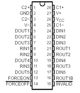 Specifications
Supply voltage range, VCC (see Note 1). . . . . . . . . . . . . . . . . . . . .. . . . −0.3 V to 6 V
Positive output supply voltage range, V+ (see Note 1) . . . . . . . . . . . . .−0.3 V to 7 V
Negative output supply voltage range, V− (see Note 1) . . . . . . . . . . . .0.3 V to −7 V
Supply voltage difference, V+ − V− (see Note 1) . . . . . . . . . . . . . . . . . . . . . . . . 13 V
Input voltage range, VI: Driver (FORCEOFF, FORCEON) . . . . . . . . . . . . −0.3 V to 6 V
Receiver . . . . . . . . . . . . . . . . . . . . . . . . . . . . . . . . . . . . . . . . . . . . . . . . .−25 V to 25 V
Output voltage range, VO: Driver. . . . . . . . . . . . . . . . . . . . . . . . . . . −13.2 V to 13.2 V
Receiver (INVALID) . . . . . . . . . . . . . . . . . . . . . . . . . . . . . .... . . .−0.3 V to VCC + 0.3 V
Package thermal impedance, JA (see Notes 2 and 3): DB package . . . . . . . . .62/W
PW package . . . . . . .. .62/W
Operating virtual junction temperature, TJ . . . . . . . . . . . . . . . . . . . . . . . . . . . . . .150
Storage temperature range, Tstg . . . . . . . . . . . . . . . . . . . . . . . . . . . . . −65 to 150
† Stresses beyond those listed under "absolute maximum ratings" may cause permanent damage to the device. These are stress ratings only, and functional operation of the device at these or any other conditions beyond those indicated under "recommended operating conditions" is not implied. Exposure to absolute-maximum-rated conditions for extended periods may affect device reliability.
NOTES: 1. All voltages are with respect to network GND.
2. Maximum power dissipation is a function of TJ(max), JA, and TA. The maximum allowable power dissipation at any allowable ambient temperature is PD = (TJ(max) − TA)/JA. Operating at the absolute maximum TJ of 150°C can affect reliability.
3. The package thermal impedance is calculated in accordance with JESD 51-7.
DescriptionThe MAX3238 consists of five line drivers, three line receivers, and a dual charge-pump circuit with ±15-kV ESD (HBM) protection pin to pin (serial-port connection pins, including GND). The device meets the requirements of TIA/EIA-232-F and provides the electrical interface between notebook and subnotebook computer applications. The charge pump and four small external capacitors allow operation from a single 3-V to 5.5-V supply. In addition, the MAX3238 includes an always-active noninverting output (ROUT1B), which allows applications using the ring indicator to transmit data while the device is powered down. These devices operate at data signaling rates up to 250 kbit/s and a maximum of 30-V/µs driver output slew rate.

 MAX3238 Data Sheet