Features: ` Single-Supply Operation Down to +4V
` 345MHz -3dB Bandwidth (MAX4311)
150MHz -3dB Bandwidth (MAX4313)
` 540V/s Slew Rate (MAX4313)
` Low 6.1mA Quiescent Supply Current
` 40ns Channel Switching Time
` Ultra-Low 10mVp-p Switching Transient
` 0.06%/0.08° Differential Gain/Phase Error
` Rail-to-Rail Outputs: Drives 150 to within 730mV of the Rails
` Input Common-Mode Range Includes Negative Rail
` Low-Power Shutdown Mode
` Available in Space-Saving 8-Pin MAX and 16-Pin QSOP PackagesApplication`Video Signal Multiplexing
`Video Crosspoint Switching
`Flash ADC Input Buffers
`75 Video Cable Drivers
`High-Speed Signal Processing
`Broadcast Video
`Medical Imaging
`Multimedia ProductsPinout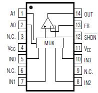 Specifications
Supply Voltage (VCC to VEE) .................................................12V
Input Voltage....................................(VEE - 0.3V) to (VCC + 0.3V)
All Other Pins ...................................(VEE - 0.3V) to (VCC + 0.3V)
Output Current.............................................................±120mA
Short-Circuit Duration (VOUT to GND, VCC or VEE)......Continuous
Continuous Power Dissipation (TA = +70°C)
8-Pin SO (derate 5.9mW/°C above +70°C)..................471mW
8-Pin MAX (derate 4.1mW/°C above +70°C) .............330mW
14-Pin SO (derate 8.3mW/°C above +70°C)................667mW
16-Pin SO (derate 8.7mW/°C above +70°C)................696mW
16-Pin QSOP (derate 8.3mW/°C above +70°C)...........667mW
Operating Temperature Range .......................-40°C to +85°C
Storage Temperature Range .........................-65°C to +150°C
Lead Temperature (soldering, 10s) ..............................+300°C
Stresses beyond those listed under "Absolute Maximum Ratings" may cause permanent damage to the device. These are stress ratings only, and functional operation of the device at these or any other conditions beyond those indicated in the operational sections of the specifications is not implied. Exposure to absolute maximum rating conditions for extended periods may affect device reliability.
DescriptionThe MAX4311 single-supply mux-amps combine high-speed operation, low-glitch switching, and excellent video specifications. The six products in this family are differentiated by the number of multiplexer inputs and the gain configuration. The MAX4310/ MAX4311/MAX4312 integrate 2-/4-/8-channel multiplexers, respectively, with an adjustable gain amplifier optimized for unity-gain stability. The MAX4313/MAX4314/ MAX4315 integrate 2-/4-/8-channel multiplexers, respectively, with a +2V/V fixed-gain amplifier. The MAX4311 has 40ns channel switching time and low 10mVp-p switching transients, making them ideal for video-switching applications. The MAX4311 operate from a single +4V to +10.5V supply, or from dual supplies of ±2V to ±5.25V, and they feature Rail-to-Rail® outputs and an input common-mode voltage range that extends to the negative supply rail.
The MAX4311 has a -3dB bandwidth of 280MHz/345MHz/265MHz and up to a 460V/s slew rate. The MAX4313/MAX4314/MAX4315, with 150MHz/127MHz/97MHz -3dB bandwidths up to a 540V/s slew rate, and a fixed gain of +2V/V, are ideally suited for driving back-terminated cables. Quiescent supply current is as low as 6.1mA, while low-power shutdown mode reduces supply current to as low as 560A and places the outputs in a high-impedance state. The MAX4311's internal amplifiers maintain an open-loop output impedance of only 8 over the full output voltage range, minimizing the gain error and bandwidth changes under loads typical of most rail-to-rail amplifiers. With differential gain and phase errors of 0.06% and 0.08°, respectively, these devices are ideal for broadcast video applications.

 MAX4311 Data Sheet