Features: · 8 Independent Output Channels
· Built-In Inductive Kickback Protection
· Drive +3V and +5V Relays
· Guaranteed 70mA (min) Coil Drive Current
· SET Function to Turn On All Outputs Simultaneously
· RESET Function to Turn Off All Outputs Simultaneously
· SPI-/QSPI-/MICROWIRE-Compatible Serial Interface (MAX4820)
· Serial Digital Output for Daisy Chaining (MAX4820)
· Parallel Interface (MAX4821)
· Low 50µA (max) Quiescent Supply Current
· Space-Saving 20-Pin Thin QFN PackageApplication·Central Office
·ATE
·DSL, ADSL Line Cards
·Industrial Equipment
·E1/T1 RedundancyPinout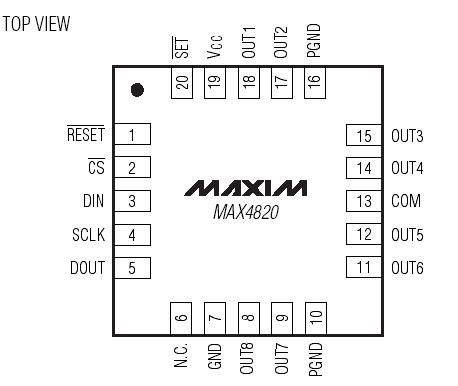 Specifications
(All voltages referenced to GND.)
VCC, COM...................................................................-0.3V to +6.0V
OUT_.............................................................-0.3V to (VCOM + 0.3V)
CS, SCLK, DIN, SET, RESET, A0, A1, A2, LVL................-0.3V to +6.0V
DOUT................................................................-0.3V to (VCC + 0.3V)
Continuous OUT_ Current (all outputs turned on) ..................150mA
Continuous OUT_ Current (single output turned on) ..............300mA
Continuous Power Dissipation (TA = +70°C)
20-Lead Thin QFN
(derate 16.9mW/°C above +70°C).....................................1350mW
JA .....................................................................................59.3°C/W
20-Pin TSSOP
(derate 21.7mW/°C above +70°C).....................................1739mW
JA ........................................................................................46°C/W
Operating Temperature Range ................................-40°C to +85°C
Junction Temperature.............................................................+150°C
Storage Temperature Range .................................-65°C to +150°C
Soldering Temperature (10s) ................................................+300°C
Stresses beyond those listed under "Absolute Maximum Ratings" may cause permanent damage to the device. These are stress ratings only, and functional operation of the device at these or any other conditions beyond those indicated in the operational sections of the specifications is not implied. Exposure to absolute maximum rating conditions for extended periods may affect device reliability.
DescriptionThe MAX4820/MAX4821 8-channel relay drivers offer built-in kickback protection and drive +3.3V/+5V nonlatching or dual-coil-latching relays. These devices are especially useful when driving +3V relays. Each independent open-drain output features a 2Ω on-resistance and is guaranteed to sink 70mA (min) of load current. Both devices consume less than 50µA (max) quiescent current and have 1µA output off-leakage current.
The MAX4820 features an SPI™-/QSPI™-/MICROWIRE™- compatible serial interface. Input data is shifted into an 8- bit shift register and latched to the outputs when CS transitions from low to high. Each data bit in the shift register corresponds to a specific output, allowing independent control of all outputs.
The MAX4820 features a 4-bit (A0, A1, A2, LVL) parallel- input interface. The first three bits (A0, A1, A2) determine the output address, and the fourth bit (LVL) determines whether the selected output is switched on or off. Data is latched to the outputs when CS transitions from low to high.
Both devices feature separate set and reset functions that allow the user to turn on or turn off all outputs simultaneously with a single control line. Built-in hysteresis (Schmidt trigger) on all digital inputs allows this device to be used with slow rising and falling signals, such as those from optocouplers or RC power-up initialization circuits. The MAX4820/MAX4821 are available in 20-pin TSSOP and space-saving 20-pin thin QFN packages.

 MAX4820 Data Sheet