Features: * ESD Protection: ±15kV-Human Body Model
* Slew-Rate Limited for Error-Free Data
Transmission (MAX483E/487E/488E/489E)
* Low Quiescent Current:
120µA (MAX483E/487E/488E/489E)
230µA (MAX1487E)
300µA (MAX481E/485E/490E/491E)
* -7V to +12V Common-Mode Input Voltage Range
* Three-State Outputs
* 30ns Propagation Delays, 5ns Skew
(MAX481E/485E/490E/491E/1487E)
* Full-Duplex and Half-Duplex Versions Available
* Allows up to 128 Transceivers on the Bus
(MAX487E/MAX1487E)
* Current Limiting and Thermal Shutdown for
Driver Overload ProtectionApplication* Low-Power RS-485 Transceivers
* Low-Power RS-422 Transceivers
* Level Translators
* Transceivers for EMI-Sensitive Applications
* Industrial-Control Local Area NetworksPinout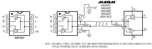 SpecificationsSupply Voltage (VCC) ................................................................12V
Control Input Voltage (RE, DE).......................-0.5V to (VCC + 0.5V)
Driver Input Voltage (DI)................................-0.5V to (VCC + 0.5V)
Driver Output Voltage (Y, Z; A, B) ..............................-8V to +12.5V
Receiver Input Voltage (A, B).....................................-8V to +12.5V
Receiver Output Voltage (RO).........................-0.5V to (VCC + 0.5V)
Continuous Power Dissipation (TA = +70)
8-Pin Plastic DIP (derate 9.09mW/ above +70) .........727mW
14-Pin Plastic DIP (derate 10.00mW/ above +70)......800mW
8-Pin SO (derate 5.88mW/ above +70)......................471mW
14-Pin SO (derate 8.33mW/ above +70)....................667mW
Operating Temperature Ranges
MAX4_ _C_ _/MAX1487EC_ A ..................................0 to +70
MAX4_ _E_ _/MAX1487EE_ A.................................-40 to +85
Storage Temperature Range .................................-65 to +160
Lead Temperature (soldering, 10sec) .................................+300DescriptionThe MAX481E, MAX483E, MAX485E, MAX487EMAX491E, and MAX1487E are low-power transceivers for RS-485 and RS-422 communications in harsh environments. Each driver output and receiver input is protected against ±15kV electrostatic discharge (ESD) shocks, without latchup. These parts contain one driver and one receiver. The MAX483E, MAX487E, MAX488E, and MAX489E feature reduced slewrate drivers that minimize EMI and reduce reflections caused by improperly terminated cables, thus allowing error-free data transmission up to 250kbps. The driver slew rates of the MAX481E, MAX485E, MAX490E, MAX491E, and MAX1487E are not limited, allowing them to transmit up to 2.5Mbps.
These transceivers draw as little as 120µA supply current when unloaded or when fully loaded with disabled drivers (see Selection Table). Additionally, the MAX481E, MAX483E, and MAX487E have a low-current shutdown mode in which they consume only 0.5µA. All parts operate from a single +5V supply.
Drivers of MAX483E are short-circuit current limited, and are protected against excessive power dissipation by thermal shutdown circuitry that places their outputs into a high-impedance state. The receiver input has a fail-safe feature that guarantees a logic-high output if the input is open circuit.
The MAX487E and MAX1487E feature quarter-unit-load receiver input impedance, allowing up to 128 transceivers on the bus. The MAX488EMAX491E are designed for fullduplex communications, while the MAX481E, MAX483E, MAX485E, MAX487E, and MAX1487E are designed for halfduplex applications. For applications that are not ESD sensitive see the pin- and function-compatible MAX481, MAX483, MAX485, MAX487MAX491, and MAX1487.

 MAX483E Data Sheet