Features: Single-Supply Operation +5V (MAX5122) +3V (MAX5123)
Built-In 10ppm/°C max Precision Bandgap Reference +2.5V (MAX5122) +1.25V (MAX5123)
SPI/QSPI/MICROWIRE-Compatible, 3-Wire Serial Interface
Pin-Programmable Shutdown Mode and Power- Up Reset (0 or Midscale Output Voltage)
Buffered Output Capable of Driving 5k100F or 420mA Loads
Space-Saving 16-Pin QSOP Package
Pin-Compatible 13-Bit Upgrades Available (MAX5132/MAX5133)
Pin-Compatible 14-Bit Upgrades Available (MAX5171/MAX5173
ApplicationIndustrial Process Control Automatic Test Equipment Digital Offset and Gain Adjustment Motion Control Microprocessor-Controlled Systems
Pinout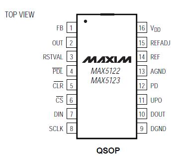 Specifications
VDD to AGND, DGND................................................-0.3V to +6V
AGND to DGND.....................................................-0.3V to +0.3V
Digital Inputs to DGND...........................................-.0.3V to +6V
Digital Outputs (DOUT, UPO) to DGND.......-0.3V to (VDD + 0.3V)
FB, OUT to AGND ......................................-0.3V to (VDD + 0.3V)
REF, REFADJ to AGND ...............................-0.3V to (VDD + 0.3V)
Maximum Current into Any Pin...........................................50mA
Continuous Power Dissipation (TA = +70)
QSOP (derate 8.00mW/ above +70).........................667mW
Operating Temperature Range ...........................-40 to +85
Storage Temperature Range .............................-65 to +150
Lead Temperature (soldering, 10sec) .............................+300
DescriptionThe MAX5122/MAX5123 low-power, 12-bit, voltage-output, digital-to-analog converters (DACs) feature an internal precision bandgap reference and output amplifier.
The MAX5122 operates on a single +5V supply with an internal +2.5V reference, and offers a configurable output amplifier. If necessary, the user can override the on-chip, <10ppm/voltage reference with an external reference. The MAX5123 has the same features as the MAX5122 but operates from a single +3V supply and has an internal +1.25V precision reference. The user-accessible inverting input and output of the amplifier allows specific gain configurations, remote sensing, and high output drive capability for a wide range of force/sense applications. Both devices draw only 500A of supply current, which reduces to 3A in power-down mode. In addition, their power-up reset feature allows for a user-selectable initial
output state of either 0V or midscale and reduces output glitches during power-up.
The serial interface is compatible with SPI™, QSPI™, and MICROWIRE™, which makes the MAX5122/MAX5123 suitable for cascading multiple devices. Each DAC has a double-buffered input organized as an input register followed by a DAC register. A 16-bit shift register loads data into the input register. The DAC register may be updated independently or simultaneously with the input register.
The MAX5122 is available in a 16-pin QSOP package and are specified for the extended-industrial (-40 to +85) operating temperature range. For pin-compatible 14-bit upgrades, see the MAX5171/MAX5173 data sheet; for the pin-compatible 13-bit version, see the MAX5132/ MAX5133 data sheet.

 MAX5122 Data Sheet