SeekIC No. : 004412271
Detail
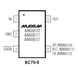
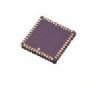
MAX8511: Features: `Space-Saving 5-Pin SC70 Package`11VRMS Output Noise at 100Hz to 100kHz Bandwidth (MAX8510)`78dB PSRR at 1kHz (MAX8510)`120mV Dropout at 120mA Load`Stable with 1F Ceramic Capacitor for Any...
 MAX8511 Data Sheet
floor Price/Ceiling Price
- Part Number:
- MAX8511
- Supply Ability:
- 5000
Price Break
- Qty
- 1~5000
- Unit Price
- Negotiable
- Processing time
- 15 Days
SeekIC Buyer Protection PLUS - newly updated for 2013!
- Escrow Protection.
- Guaranteed refunds.
- Secure payments.
- Learn more >>
Month Sales
268 Transactions
Payment Methods
All payment methods are secure and covered by SeekIC Buyer Protection PLUS.
Notice: When you place an order, your payment is made to SeekIC and not to your seller. SeekIC only pays the seller after confirming you have received your order. We will also never share your payment details with your seller.