Features: Circuit Footprint of 0.31in2
Low-Profile Design
On-Chip Power MOSFETs
High-Efficiency Switch-Mode Design
Ripple Cancellation for Low Noise
Direct Current Control Prevents TEC Current Surges
5% Accurate Adjustable Heating/Cooling Current Limits
2% Accurate TEC Voltage Limit
No Dead Zone or Hunting at Low Output Current
ITEC Monitors TEC Current
1% Accurate Voltage Reference
Switching Frequency Up to 1MHz
Synchronization (MAX8521)ApplicationSFF/SFP Modules
Fiber-Optic Laser Modules
Fiber-Optic Network Equipment
ATE
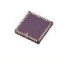
Biotech Lab EquipmentPinout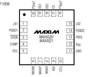 Specifications
ABSOLUTE MAXIMUM RATINGS
VDD to GND.........................................................-0.3V to +6V
SHDN, MAXV, MAXIP, MAXIN
CTLI to GND.........................................................-0.3V to +6V
COMP, FREQ, OS1, OS2, CS, REF,
ITEC to GND...........................................-0.3V to (VDD + 0.3V)
PVDD1, PVDD2 to GND.........................-0.3V to (VDD + 0.3V)
PVDD1, PVDD2 to VDD ....................................-0.3V to +0.3V
PGND1, PGND2 to GND .......................................-0.3V to +0.3V
COMP, REF, ITEC Short to GND ..................................Indefinite
LX Current (Note 1) ....................................±2.25A LX Current
Continuous Power Dissipation (TA = +70°C)
20-Pin 5mm x 5mm x 0.9mm QFN (derate 20.8mW/°C
above +70°C) (Note 2)...................................................1.67W
3mm x 3mm UCSP (derate 22mW/°C
above +70°C).................................................................1.75W
Maximum Junction Temperature ....................................+150°C
Storage Temperature Range .........................-65°C to +150°C
Lead Temperature (soldering 10s) ................................+300°C
Stresses beyond those listed under "Absolute Maximum Ratings" may cause permanent damage to the device. These are stress ratings only, and functional operation of the device at these or any other conditions beyond those indicated in the operational sections of the specifications is not implied. Exposure to absolute maximum rating onditions for extended periods may affect device reliability.
Note 1: LX has internal clamp diodes to PGND and PVDD. Applications that forward bias these diodes should take care not to exceed the IC's package power dissipation limits.
Note 2: Solder underside metal slug to PC board ground plane.
DescriptionThe MAX8520/MAX8521 are designed to drive thermoelectric coolers (TECs) in space-constrained optical modules. Both devices deliver ±1.5A output current and control the TEC current to eliminate harmful current surges. On-chip FETs MAX8521 minimize external components and high switching frequency reduces the size of external components.
The MAX8520 and MAX8521 operate from a single supply and bias the TEC between the outputs of two synchronous
buck regulators. This operation allows for temperature control without "dead zones" or other nonlinearities at low current. This arrangement ensures that the control system does not hunt when the set point of MAX8521 is very close to the natural operating point, requiring a small amount of heating or cooling. An analog control signal precisely sets the TEC current.
MAX8521 feature accurate, individually adjustable heating current limit and cooling current limit, along with maximum TEC voltage limit to improve the reliability of optical modules. An analog output signal monitors the TEC current. A unique ripple cancellation scheme of MAX8521 helps reduce noise.
The MAX8520 is available in a 5mm x 5mm thin QFN package and its switching frequency is adjustable up to 1MHz through an external resistor. The MAX8521 is also available in a 5mm x 5mm thin QFN, as well as a spacesaving 3mm x 3mm UCSP™, with a pin-selectable switching frequency of 500kHz or 1MHz.

 MAX8521 Data Sheet