Features: ` Comparator + Precision Reference in SOT23
` +2.5V to +5.5V Single-Supply Operation (MAX9040MAX9043)
` Low Supply Current (MAX9040/MAX9050)
40A Quiescent
50A with 100kHz Switching
` 400ns Propagation Delay
` Rail-to-Rail Inputs
` Rail-to-Rail Output Stage Sinks and Sources 8mA
` Internal ±3mV Hysteresis
` Voltage Reference Offers
±0.4% max Initial Accuracy (A grade)
6ppm/°C typ Temperature Coefficient (A grade)
Stable for 0nF to 4.7nF Capacitive LoadsApplication· Precision Battery Management
· Window Comparators
· IR Receivers
· Level Translators
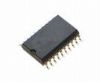
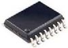
· Digital Line ReceiversPinout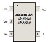 Specifications
Supply Voltage (VCC to VEE) ....................................-0.3V to +6V
All Other Pins ...................................(VEE - 0.3V) to (VCC + 0.3V)
Output Short-Circuit Duration
(OUT_, REF) ..................Indefinite Short Circuit to Either Supply
Continuous Power Dissipation (TA = +70°C)
5-Pin SOT23 (derate 7.10mW/°C above +70°C)............571mW
6-Pin SOT23 (derate 8.70mW/°C above +70°C)............696mW
8-Pin MAX (derate 4.1mW/°C above +70°C) ...............330mW
10-Pin MAX (derate 5.6mW/°C above +70°C) .............444mW
8-Pin SO (derate 5.88mW/°C above +70°C)..................471mW
Operating Temperature Range ........................-40°C to +85°C
Junction Temperature....................................................+150°C
Storage Temperature Range ..........................-65°C to +150°C
Lead Temperature (soldering, 10s) ..............................+300°C
Stresses beyond those listed under "Absolute Maximum Ratings" may cause permanent damage to the device. These are stress ratings only, and functional operation of the device at these or any other conditions beyond those indicated in the operational sections of the specifications is not implied. Exposure to absolute maximum rating conditions for extended periods may affect device reliability.
DescriptionThe MAX9040MAX9043 and MAX9050MAX9053 feature combinations of low-power comparators and precision voltage references. Their operating voltage range makes them ideal for both +3V and +5V systems. The MAX9040/MAX9041/MAX9050/MAX9051 have a single comparator and reference consuming only 40A of supply current. The MAX9042/MAX9043/MAX9052/MAX9053 have dual comparators and one reference, and consume only 55A of supply current. Low-voltage operation and low supply current make these devices ideal for battery-operated systems.
The comparators MAX9040 feature Rail-to-Rail® inputs and outputs, with a common-mode input voltage range that extends 250mV beyond the supply rails. Input bias current is typically 1.0pA, and input offset voltage is typically 0.5mV. Internal hysteresis ensures clean output switching, even with slow-moving input signals. The output stage of MAX9040 features a unique design that limits supply current surges while switching, virtually eliminating supply glitches typical of many other comparators. This design also minimizes overall power consumption under dynamic conditions. The comparator MAX9040 outputs have rail-to-rail push-pull output stages that sink and source up to 8mA. The propagation delay is 400ns, even with the low operating supply current.
The reference output voltage is set to 2.048V in the MAX9040MAX9043 and to 2.500V in the MAX9050MAX9053. These devices are offered in two grades: an A grade with 0.4% initial accuracy and 6ppm/°C tempco, and a B grade with 1% initial accuracy and 100ppm/°C tempco. The voltage reference of MAX9040 features a proprietary curvature-correction circuit and lasertrimmed thin-film resistors. The series-mode references can sink or source up to 500A of load current.

 MAX9040 Data Sheet