Features: Integrated Termination Eliminates Four External
Resistors (MAX9126)
Pin Compatible with DS90LV032A
Guaranteed 500Mbps Data Rate
300ps Pulse Skew (max)
Conform to ANSI TIA/EIA-644 LVDS Standard
Single +3.3V Supply
Low 70µAShutdown Supply Current
Fail-Safe CircuitApplicationDigital Copiers
Laser Printers
Cellular Phone Base Stations
Add/Drop Muxes
Digital Cross-Connects
DSLAMs
Network Switches/Routers
Backplane Interconnect
Clock DistributionPinout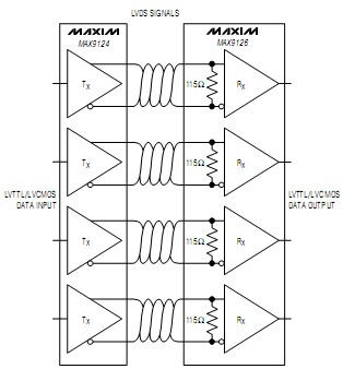 Specifications
VCC to GND............................................................-0.3V to +4.0V
IN_+, IN_- to GND..................................................-0.3V to +4.0V
EN, ENto GND................................................-0.3V to (VCC+ 0.3V)
OUT_ to GND.................................................-0.3V to (VCC+ 0.3V)
Continuous Power Dissipation (TA= +70°C)
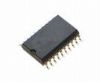
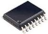
16-Pin TSSOP (derate 9.4mW/°C above +70°C)...............755mW
16-Pin SO (derate 8.7mW/
°C above +70°C)..............................................................696mW
Storage Temperature Range..............................-65°C to +150°C
Maximum Junction Temperature........................................+150°C
Operating Temperature Range.............................-40°C to +85°C
Lead Temperature (soldering, 10s)...................................+300°C
ESD Protection (Human Body Model) IN_+, IN_-, OU..........±7.5kV
DescriptionThe MAX9125/MAX9126 quad low-voltage differential signaling (LVDS) line receivers are ideal for applica- tions requiring high data rates, low power, and reduced noise. The MAX9125/MAX9126 are guaranteed to receive data at speeds up to 500Mbps (250MHz) over controlled-impedance media of approximately 100 Ω.The transmission media may be printed circuit (PC) board traces or cables. The MAX9125/MAX9126 accept four LVDS differential inputs and translate them to 3.3V CMOS outputs.
The MAX9126 features integrated parallel termination resis- tors (nominally 115Ω), which eliminate the requirementfor four discrete termination resistors and reduce stublength. The MAX9125 inputs are high impedance and require an external termination resistor when used in apoint-to-point connection.
The MAX9126 support a wide common-mode input range of 0.05V to 2.35V, allowing for ground potential differ- ences and common-mode noise between the driver and the receiver. A fail safe feature of MAX9126 sets the output high when the inputs are open, or when the inputs are undriven and shorted or parallel terminated. The EN and ENinputs control the high-impedance output and are common to all four receivers. Inputs conform to the ANSI TIA/EIA-644 LVDS standard. The MAX9125/ MAX9126 operate from a single +3.3V supply, are specified for operation from -40°C to +85°C, and are available in 16-pin TSSOP and SO packages. Refer to the MAX9124 data sheet for a quad LVDS line driver.

 MAX9126 Data Sheet