Features: ` No Bulky DC-Blocking Capacitors Required
` Low-Power Shutdown Mode, < 0.1A
` Adjustable Gain (MAX9728A) or Fixed -1.5V/V Gain (MAX9728B)
` Low 0.02% THD+N
` High PSRR (80dB at 1kHz) Eliminates LDO
` Integrated Click-and-Pop Suppression
` 4.5V to 5.5V Single-Supply Operation
` Low Quiescent Current (3.5mA)
` Available in Space-Saving Packages
12-Pin Thin QFN (3mm x 3mm x 0.8mm)
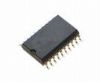
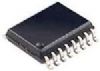
14-Pin TSSOP (5mm x 4.4mm x 1.1mm)Application·Notebook PCs
·DVD Players
·LCD/PDP Displays
·CRT TVs
·Multimedia MonitorsSpecificationsVDD to GND........................................................-0.3V to +6V
PVSS to SVSS ..................................................-0.3V to +0.3V
PGND to SGND ................................................-0.3V to +0.3V
C1P to PGND.........................................-0.3V to (VDD + 0.3V)
C1N to PGND.......................................(PVSS - 0.3V) to +0.3V
PVSS and SVSS to PGND.....................................-6V to +0.3V
IN_ to SGND (MAX9728A)......................-0.3V to (VDD + 0.3V)
IN_ to SGND (MAX9728B)..........(SVSS - 0.3V) to (VDD + 0.3V)
OUT_ to SVSS (Note 1)..-0.3V to Min (VDD - SVSS + 0.3V, +9V)
OUT_ to VDD (Note 2) ...+0.3V to Max (SVSS - VDD - 0.3V, -9V)
SHDN to _GND.....................................................-0.3V to +6V
OUT_ Short Circuit to GND ....................................Continuous
Short Circuit between OUTL and OUTR .................Continuous
Continuous Input Current into PVSS.............................260mA
Continuous Input Current (any other pin) ...................±20mA
Continuous Power Dissipation (TA = +70°C)
12-Pin TQFN (derate 14.7mW/°C above +70°C) ....1177mW
14-Pin TSSOP (derate 9.1mW/°C above +70°C) ......727mW
Operating Temperature Range ......................-40°C to +85°C
Storage Temperature Range ........................-65°C to +150°C
Junction Temperature....................................................+150°C
Lead Temperature (soldering, 10s) ..............................+300°C
Note 1: OUTR and OUTL should be limited to no more than 9V above SVSS, or above VDD + 0.3V, whichever limits first.
Note 2: OUTR and OUTL should be limited to no more than 9V below VDD, or below SVSS - 0.3V, whichever limits first.
Stresses beyond those listed under "Absolute Maximum Ratings" may cause permanent damage to the device. These are stress ratings only, and functional operation of the device at these or any other conditions beyond those indicated in the operational sections of the specifications is not implied. Exposure to absolute maximum rating conditions for extended periods may affect device reliability.
DescriptionThe MAX9728A/MAX9728B stereo headphone amplifiers are designed for display and notebook applications or portable equipment where board space is at a premium. These devices use a unique, patented DirectDrive™ architecture to produce a ground-referenced output from a single supply, eliminating the need for large DC-blocking capacitors, saving cost, board space, and component height. The MAX9728A offers an externally adjustable gain, while the MAX9728B has an internally preset gain of -1.5V/V. The MAX9728A/MAX9728B deliver up to 60mW per channel into a 32 load and have low 0.02% THD+N. An 80dB at 1kHz power-supply rejection ratio (PSRR) allows these devices to operate from noisy digital supplies without an additional linear regulator. Comprehensive clickand- pop circuitry suppresses audible clicks and pops on startup and shutdown.
The MAX9728A/MAX9728B operate from a single 4.5V to 5.5V supply, consume only 3.5mA of supply current,feature short-circuit and thermal-overload protection,and are specified over the extended -40°C to +85°C temperature range. The MAX9728B are available in tiny 12-pin Thin QFN (3mm x 3mm x 0.8mm) and 14-pin TSSOP packages (5mm x 4.4mm x 1.1mm).

 MAX9728B Data Sheet